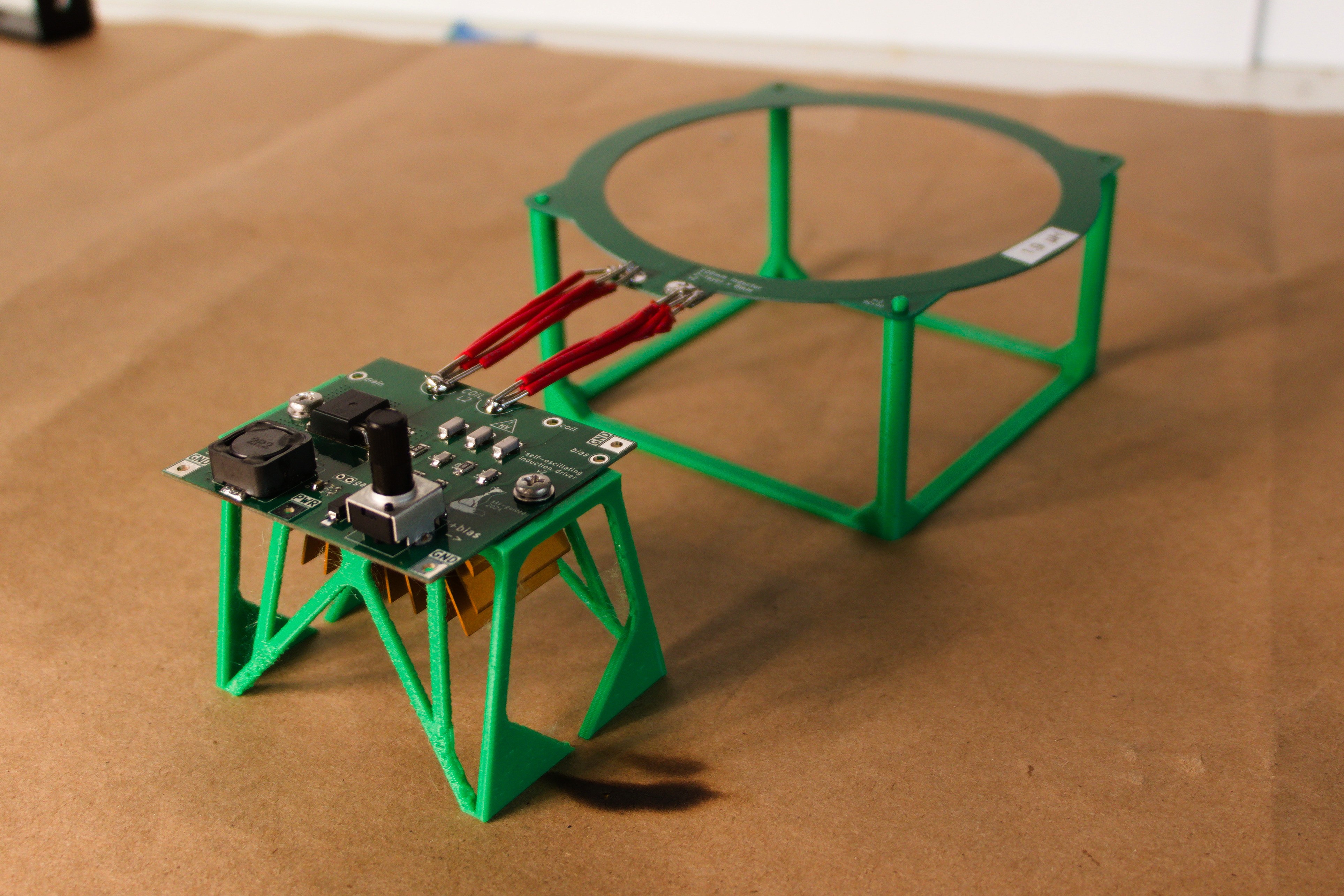
 sky-guided
A quick video demo
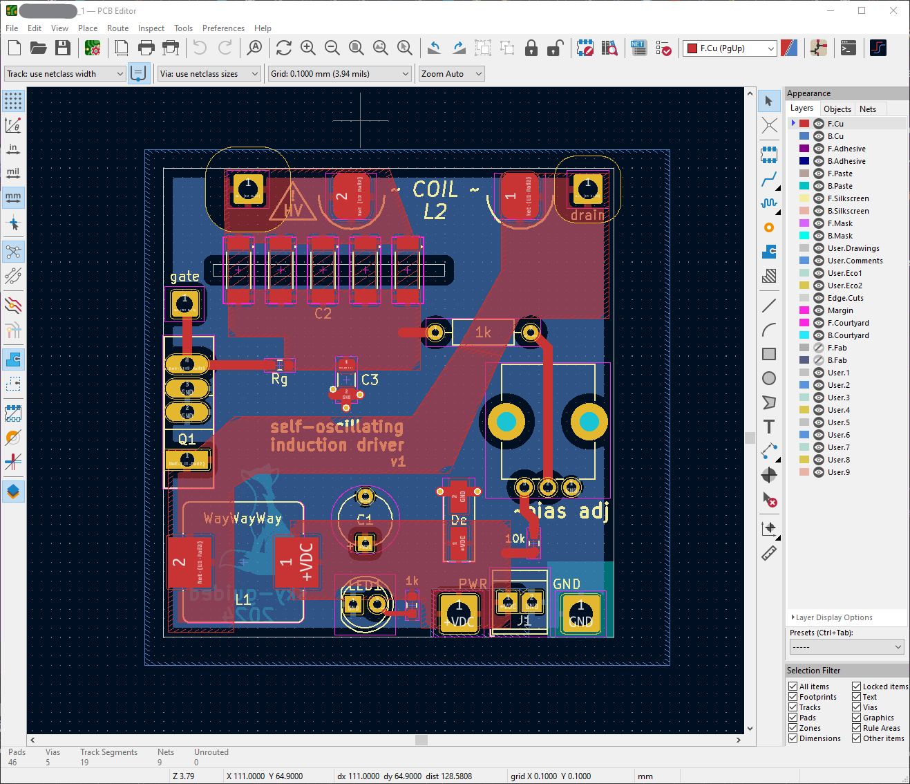
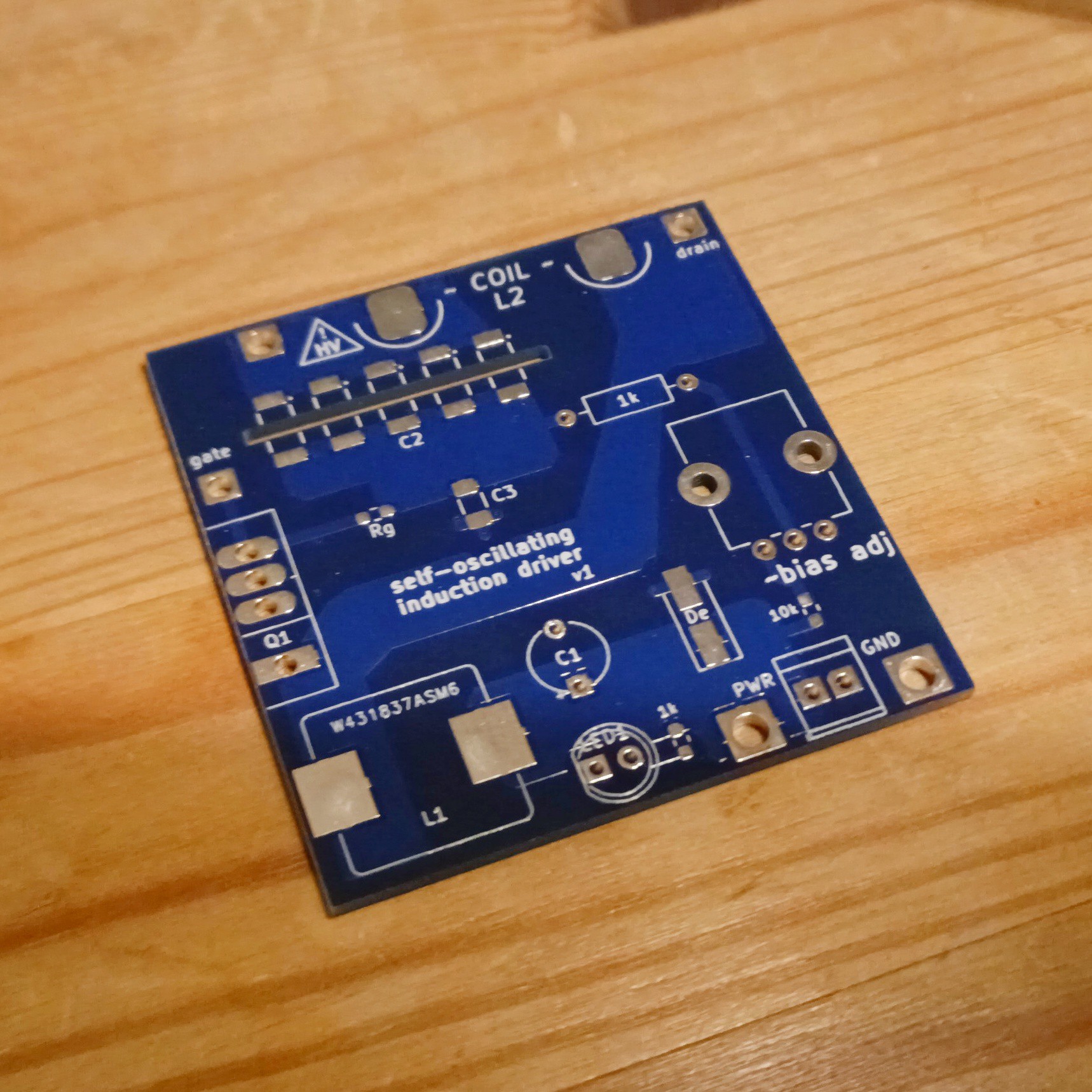
How does the driver work?
Steve Ward explains the circuit's function in terms of what happens on each cycle. That can be a useful way to think about things, but for myself I gained far more intuition about how things work by deconstructing the entire resonator into a series of functional building blocks.
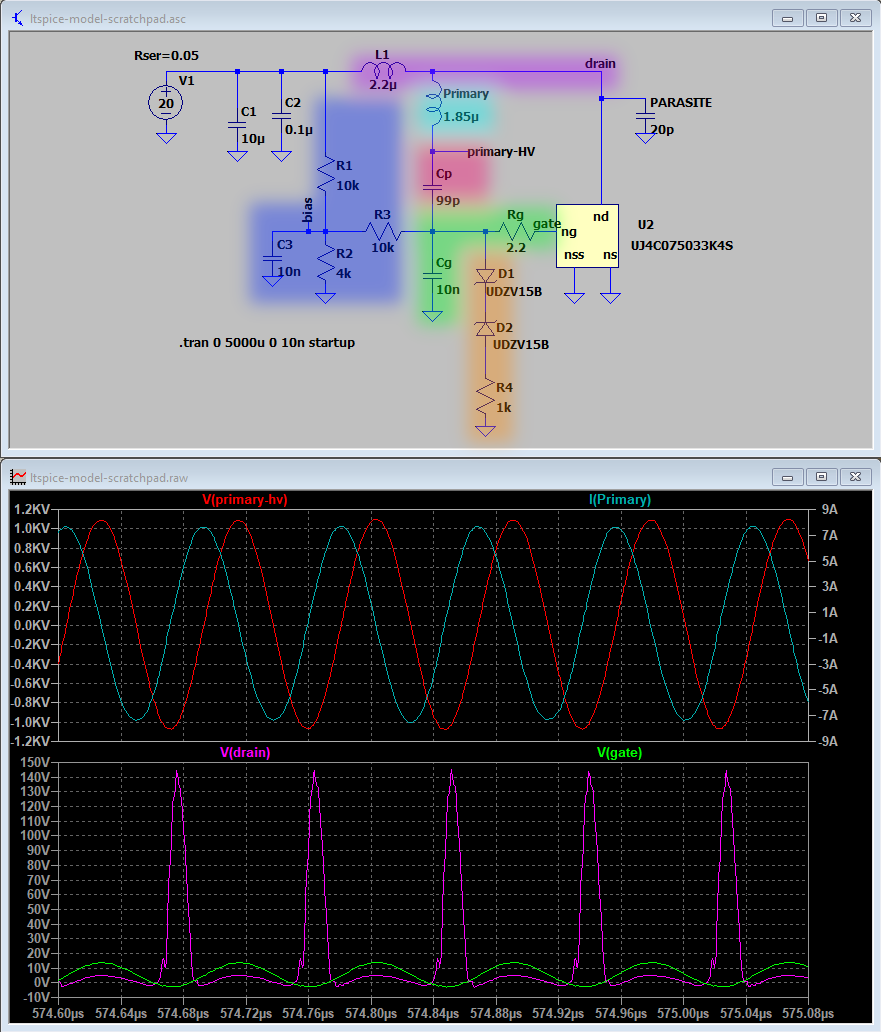
Let's start simple -- take some voltage in (V1), put an inductor (L1) in series with an N-channel mosfet (U2), and feed the mosfet a square wave at some frequency. Areas of the circuit have been highlighted to correspond to the LTspice simulation traces. (Don't worry too much about the specific values on each axis; the overall shape of each trace is more important.)
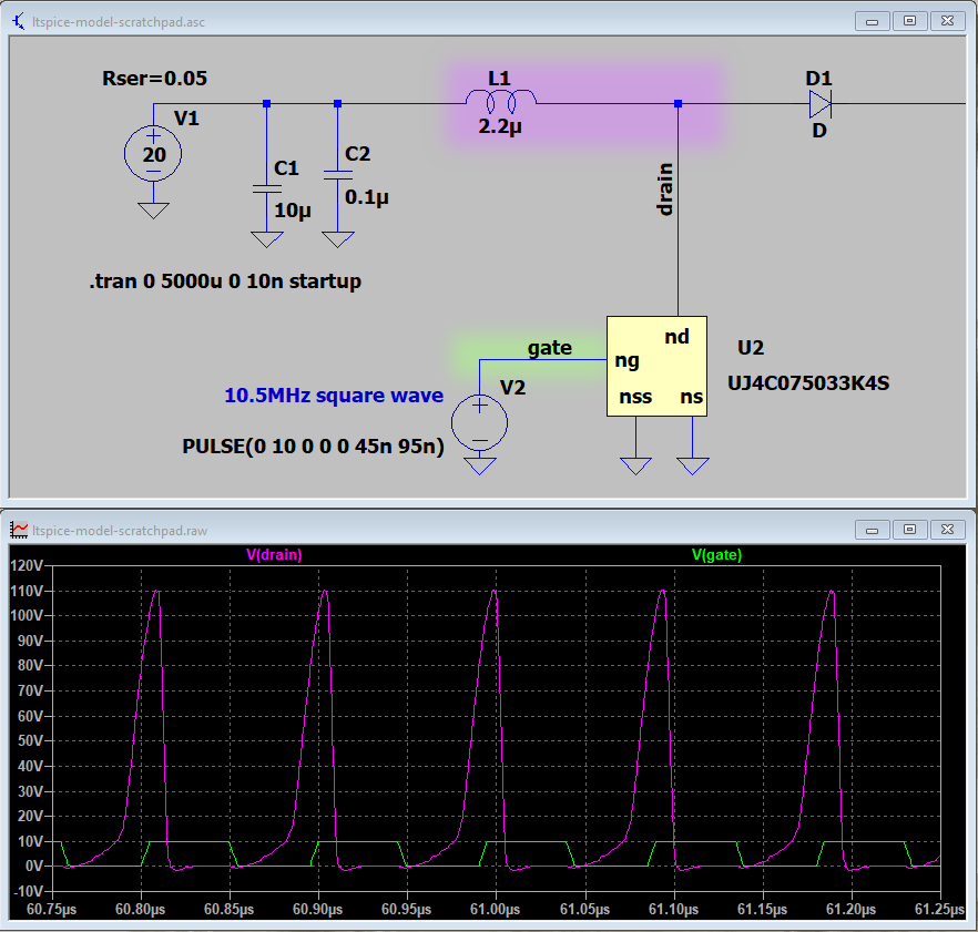
It's a boost converter!
While the mosfet is conducting, current flows through L1 and builds up a surrounding magnetic field. When the mosfet turns off, this field tries to keep shoving current through L1, resulting in a spike in voltage.
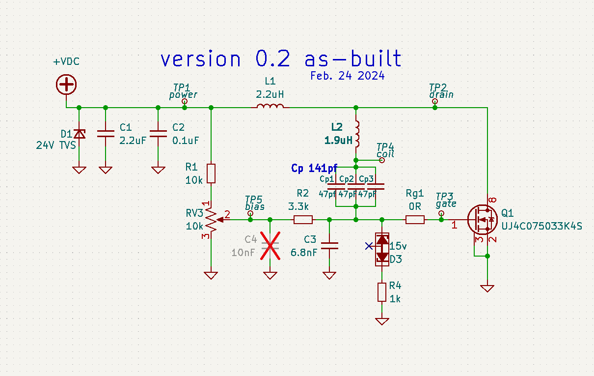
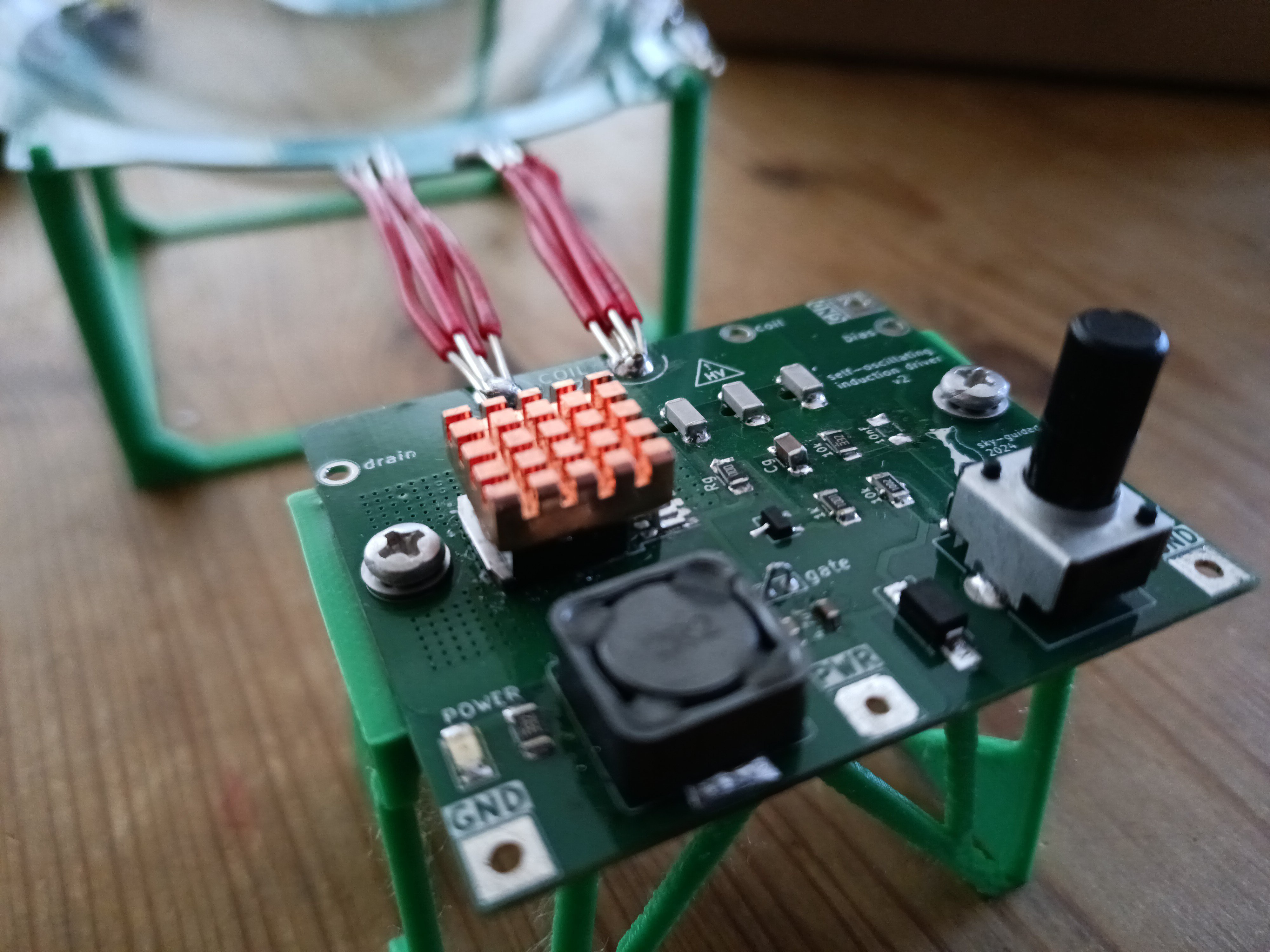
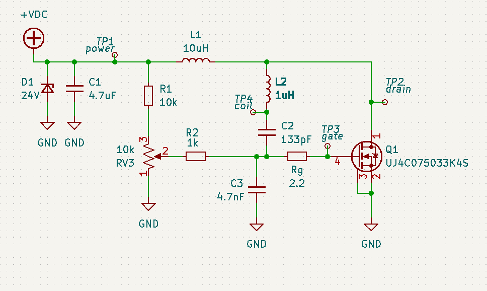
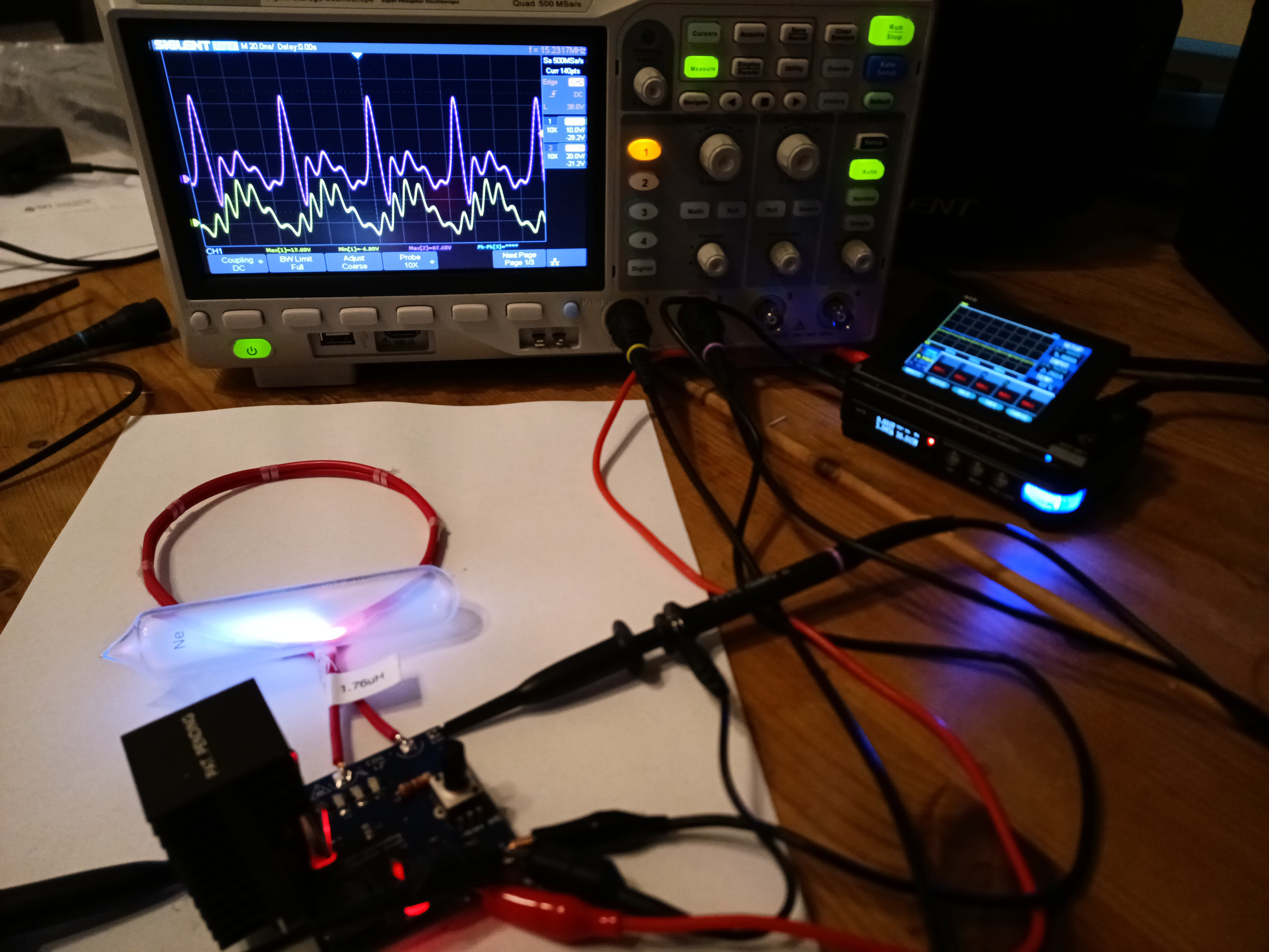
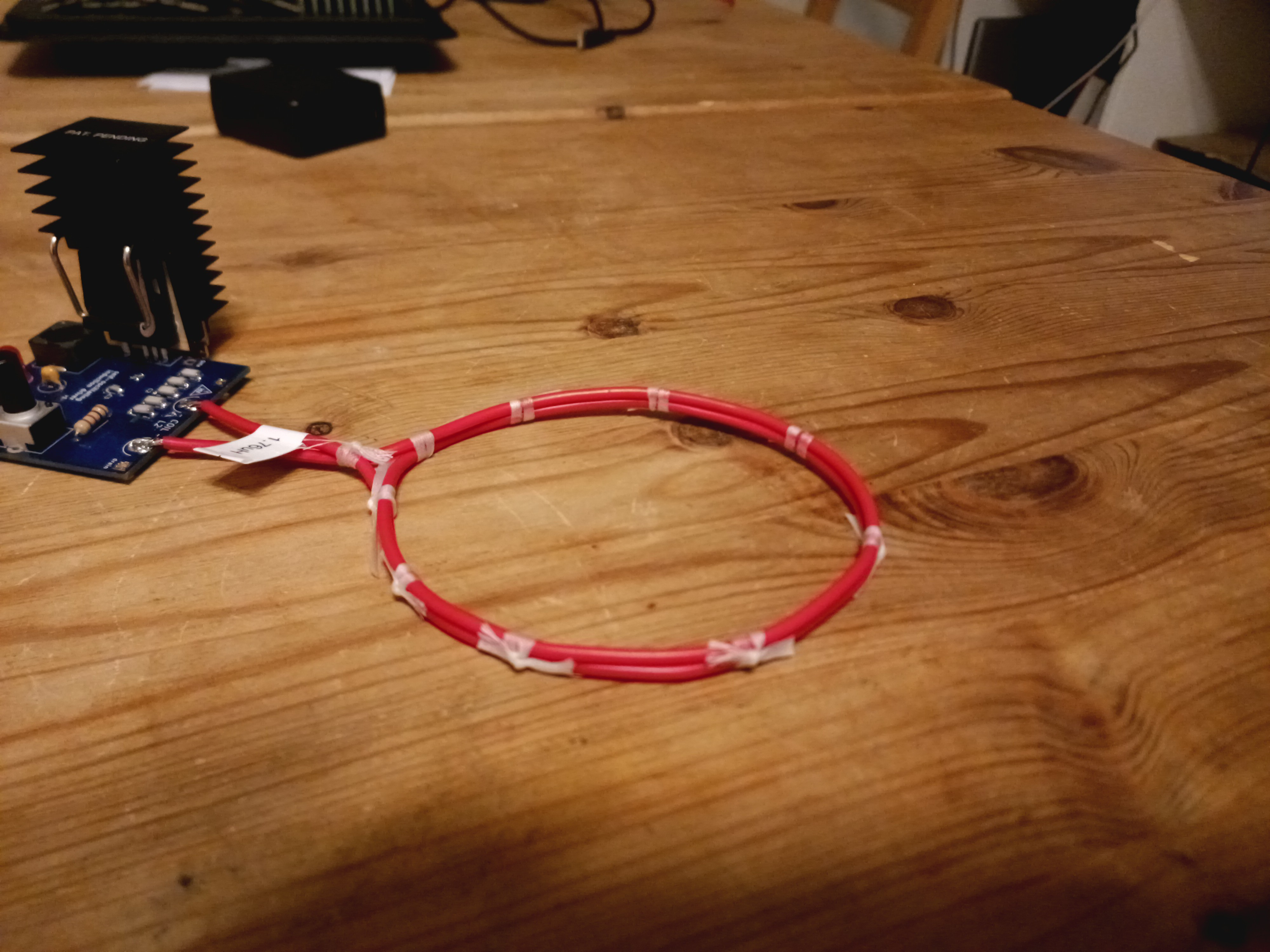
The next building block the beating heart of this project -- a resonant LC tank circuit formed by our primary inductor and a small bank of high-voltage capacitors (Cp).
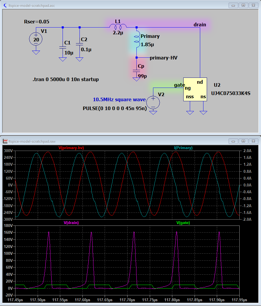
In this classic LC Resonator tank circuit, energy sloshes back and forth between the electric field in the capacitor and the magnetic field around the inductor. This resonator tank is being fed by the voltage spikes created by L1.
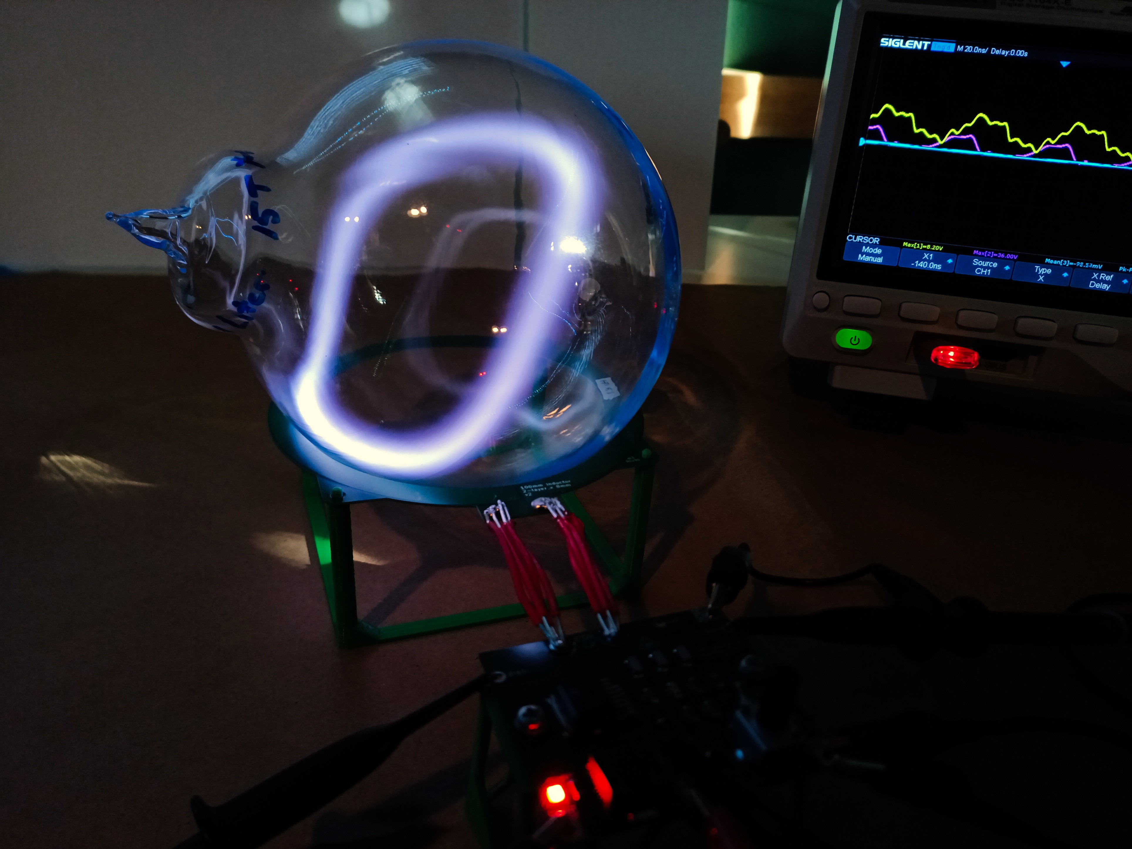
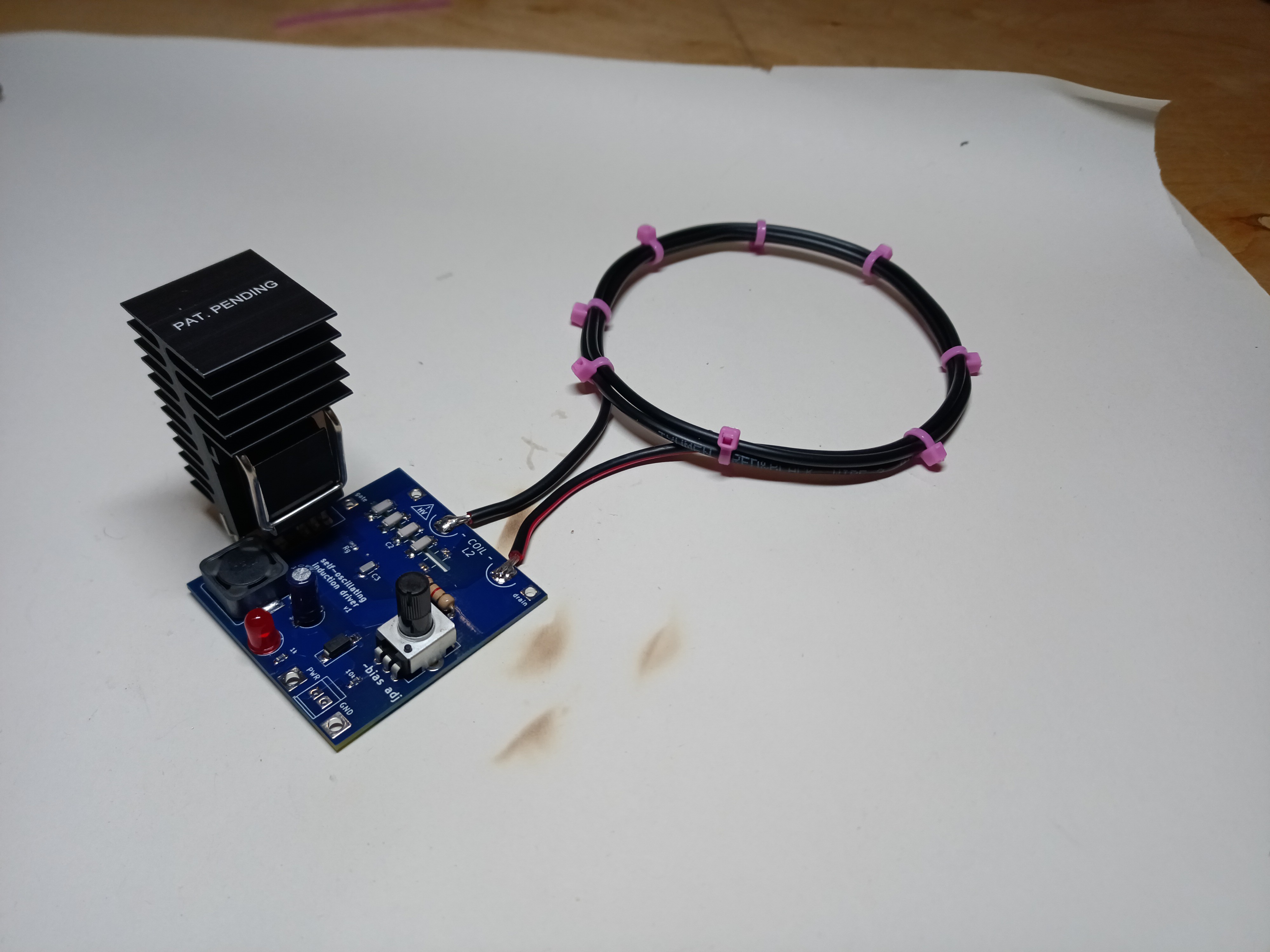
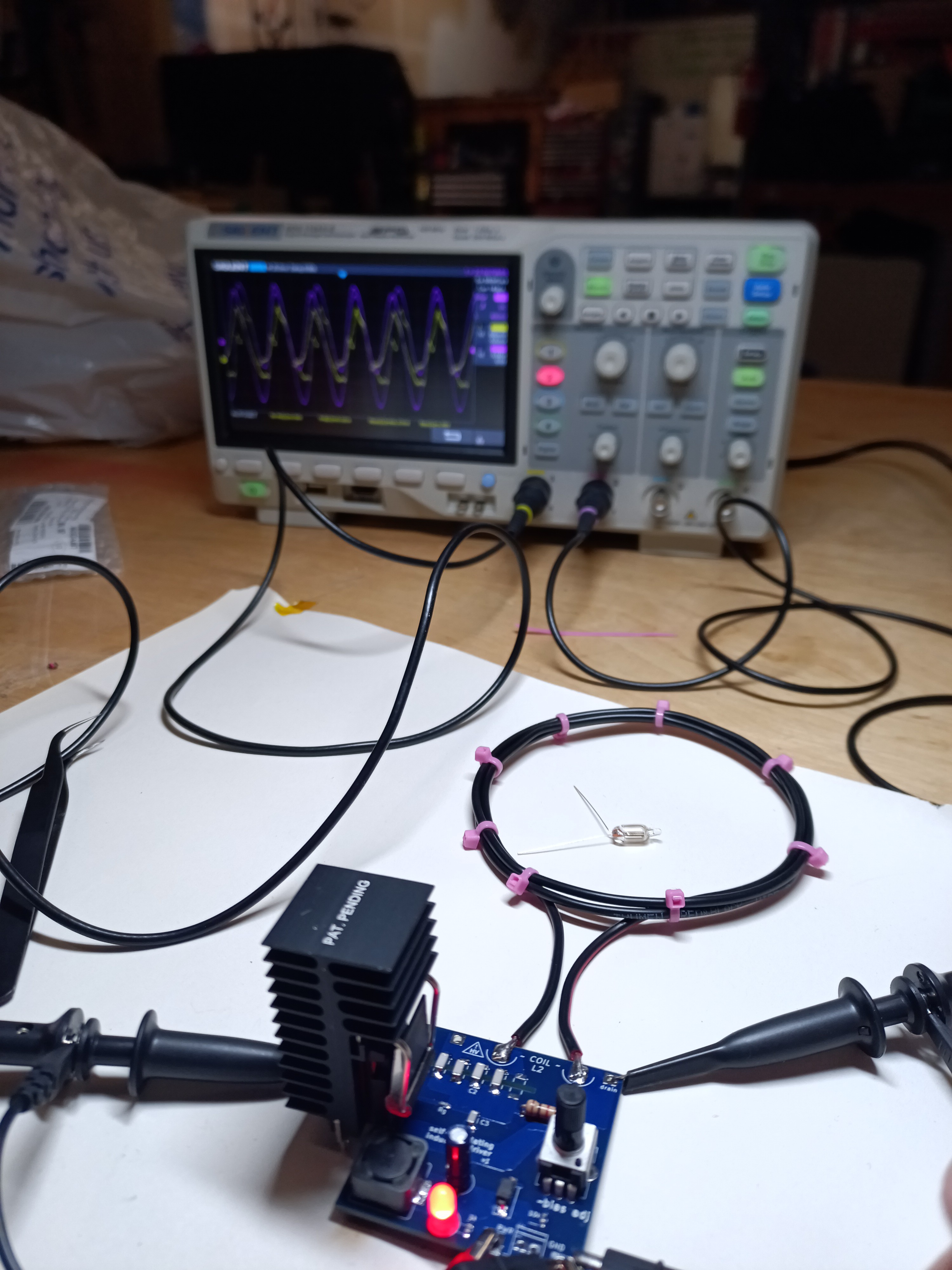
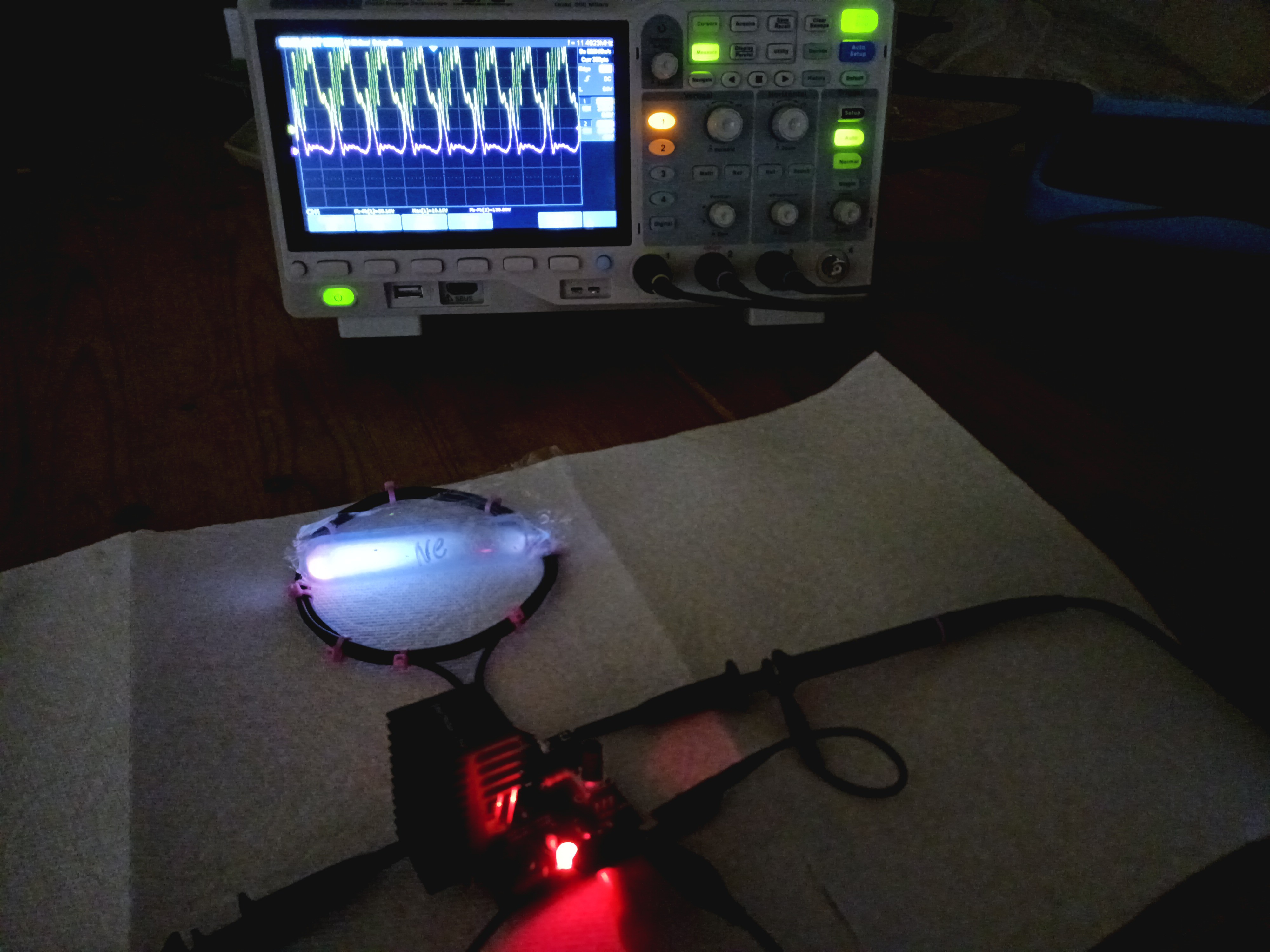
If the tank is driven by a frequency that's well-matched to its natural resonant frequency 1 / ( 2pi √(LC) ), total energy in the resonator accumulates and can greatly exceed the input on any one cycle. The primary inductor's substantial electromagnetic field will excite our xenon.
Trying to precisely match the resonator and gate drive frequencies to match each other sounds annoying and fiddly, so let's use a feedback network instead.
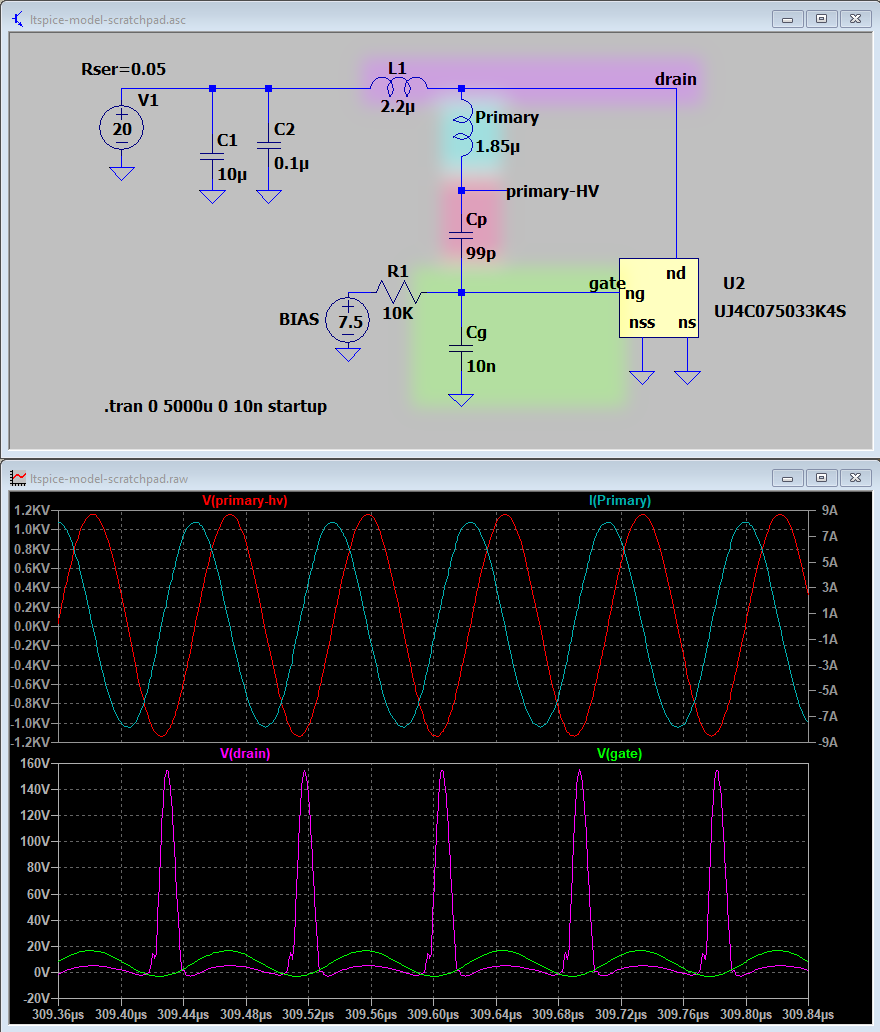
Adding a capacitor Cg (between Cp and ground) forms a capacitive voltage divider. This drives the gate at exactly the natural resonant frequency of the tank circuit. Now the tank is oscillating at 9 amps and (peak-peak) 2.4kV!
Since a capacitive voltage divider only responds to AC, the DC component of the gate drive is set by connecting some bias voltage V(bias) through a resistor. The value of Cg is chosen such that the AC amplitude at the mosfet gives solid turn-on / turn-off without exceeding operational limits, and the mosfet duty cycle is determined by where V(bias) positions this waveform relative to the mosfet's gate threshold voltage.
Rather than plonking down a magic reference voltage for V(bias), let's instead pull a voltage divider down from our supply voltage.
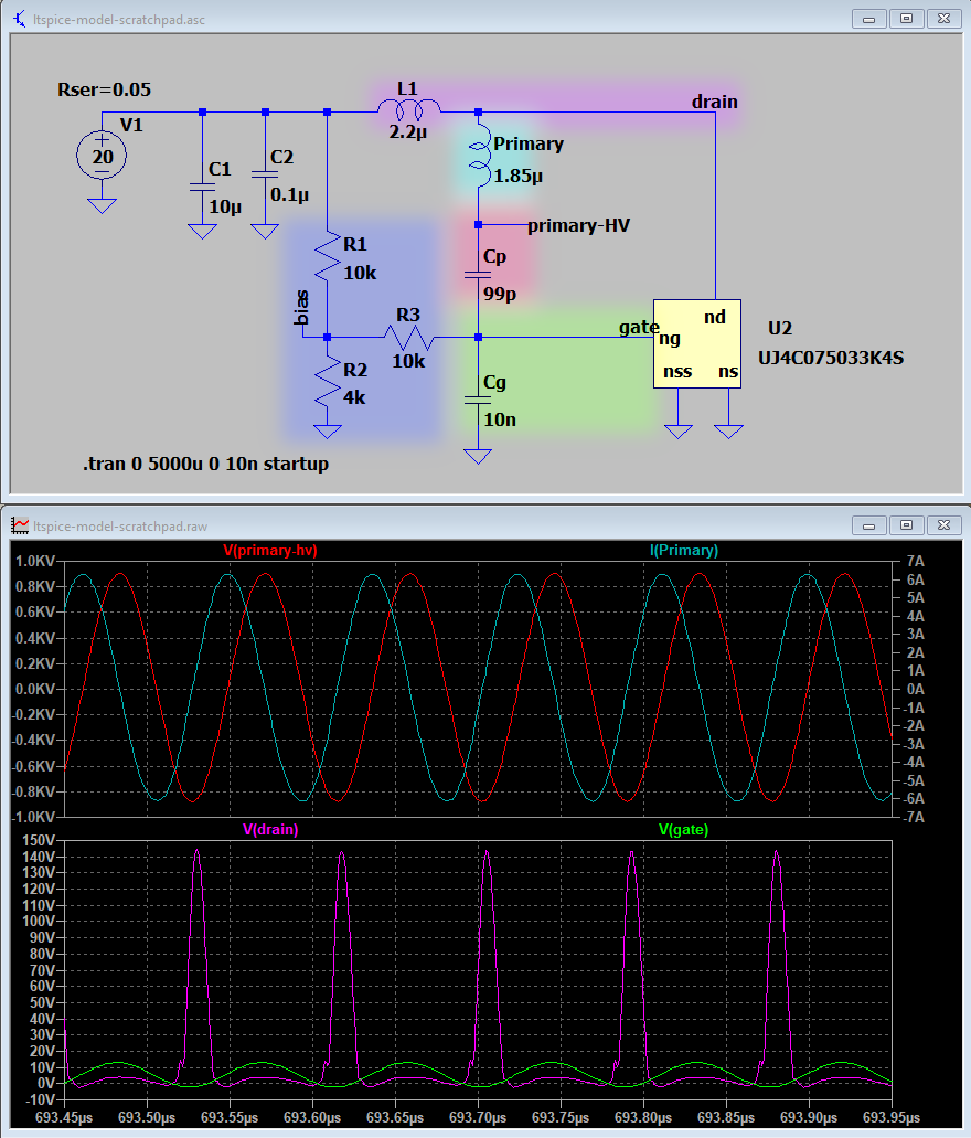
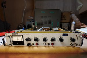
In a physical circuit, let's make R2 a potentiometer so we can freely adjust V(bias) while the circuit is in operation.
The only thing left is to fine-tune the gate drive!
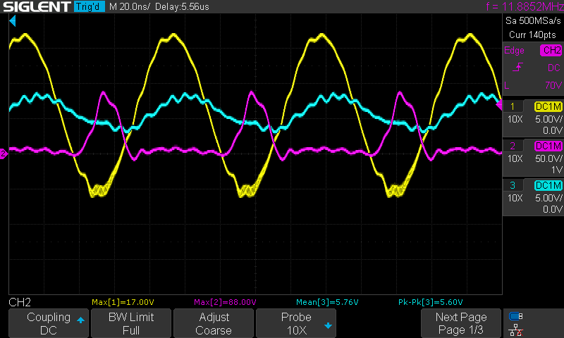
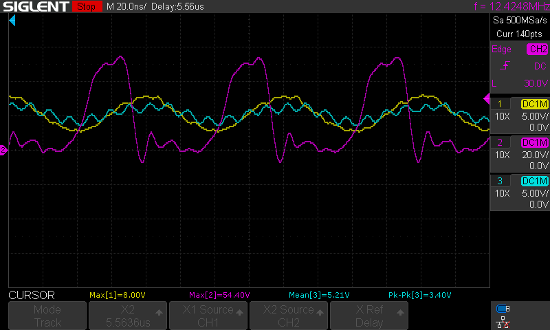
For the real circuit, it is very important that mosfet turn-off occur when the drain voltage is at a minimum, aka "zero-voltage switching" (ZVS) or "soft switching". This is complicated by the fact that the mosfet has non-neglectable internal parasitic capacitances between each of its pins. In particular, any residual energy stored in the internal capacitance C(oss) is shorted through the mosfet body at turn-on.
Lots of circuits do just fine without soft switching, but it's more typical to drive mosfets with a square wave which reduces switching losses. We're also running at >10MHz though, so even a few microjoules of lost energy per cycle can result in the mosfet soaking up tens of watts worth of waste heat. Additionally, hard switching can cause drain and/or gate voltage ringing which isn't ideal either. These effects are more than capable of causing the mosfet to self-destruct.
R(g) creates an RC circuit which introduces a phase delay on the gate. This is in addition to the phase delay cause by the time taken to charge the mosfet parasitic gate capacitance. The exact value needs to be tuned to the as-built circuit -- 2.2Ω is a placeholder. R(g) also...
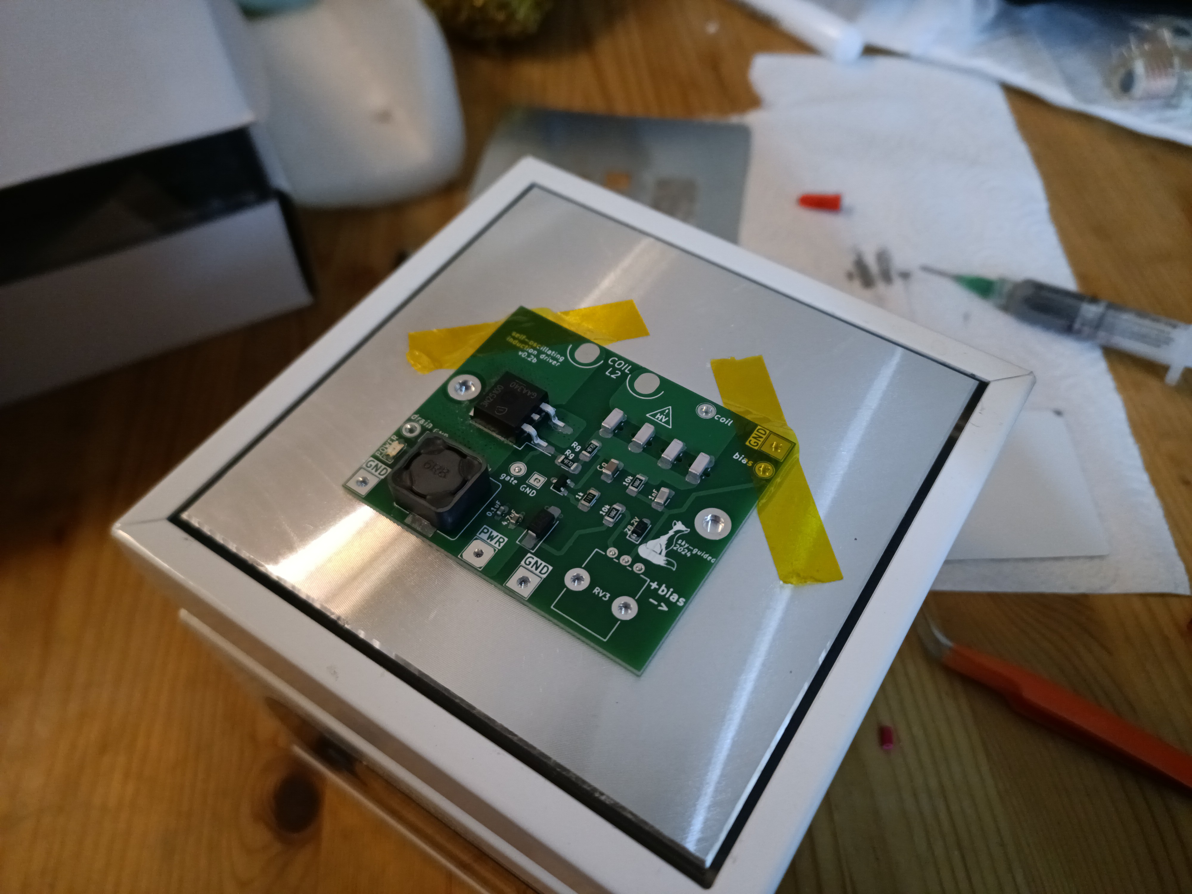
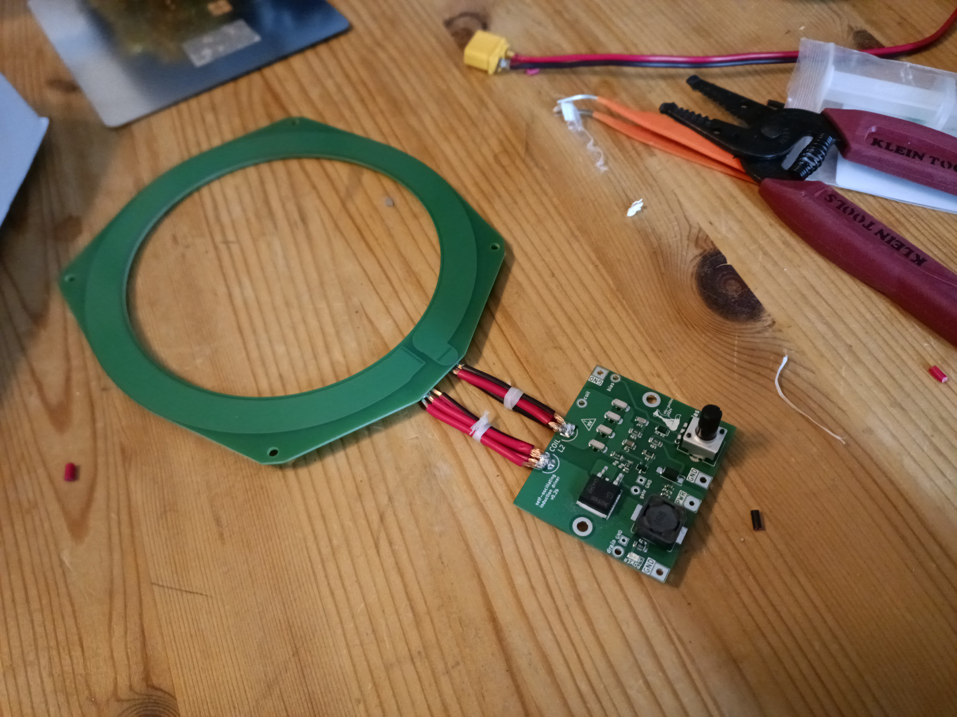
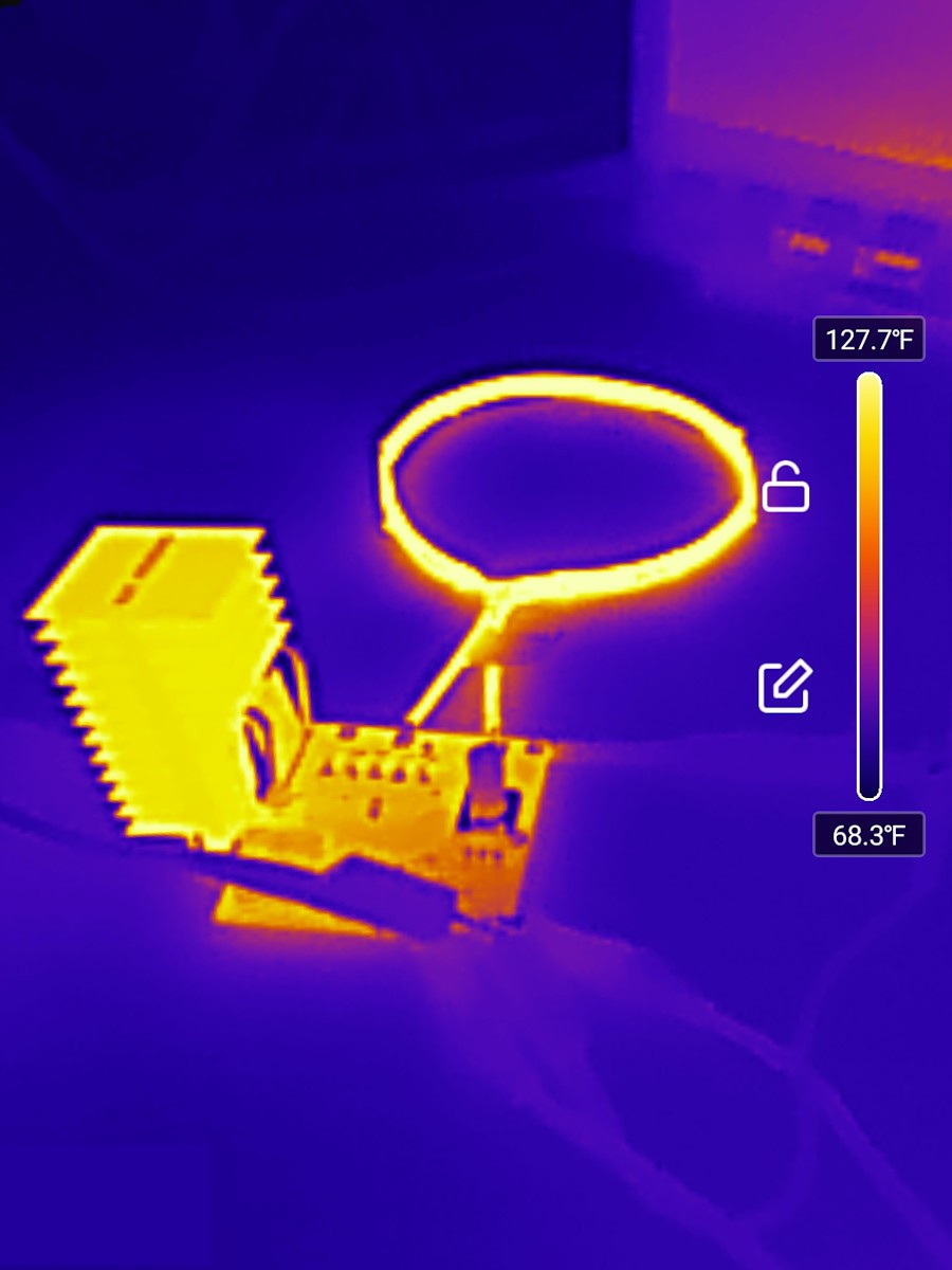
 With all of the changes, I was able to get temperatures to stabilize at ~100-110C on the mosfet body and ~50-60C on the coil while the toroid was active.
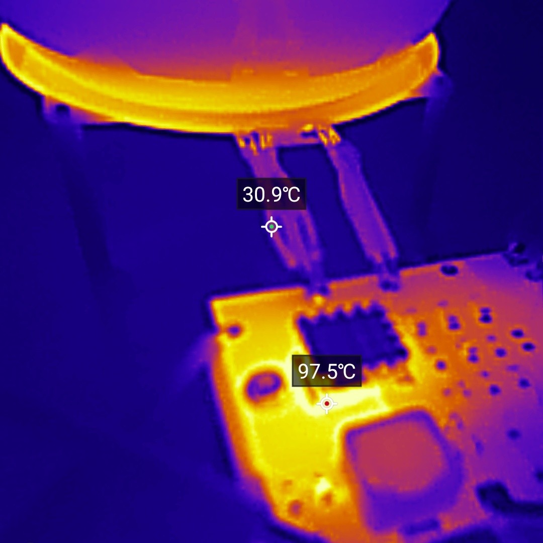 That's hotter than...
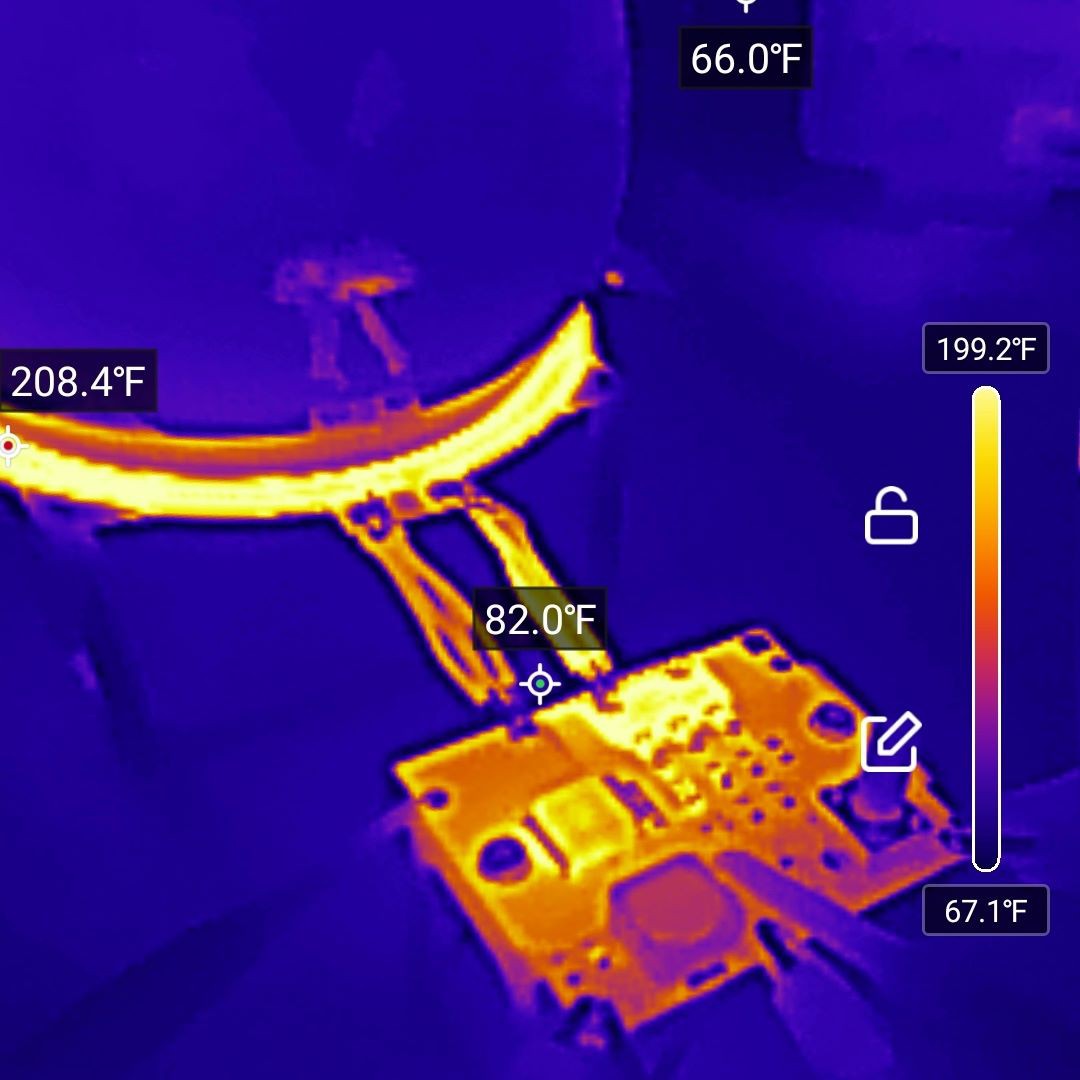
 (and i blew up zero mosfets in the process!)
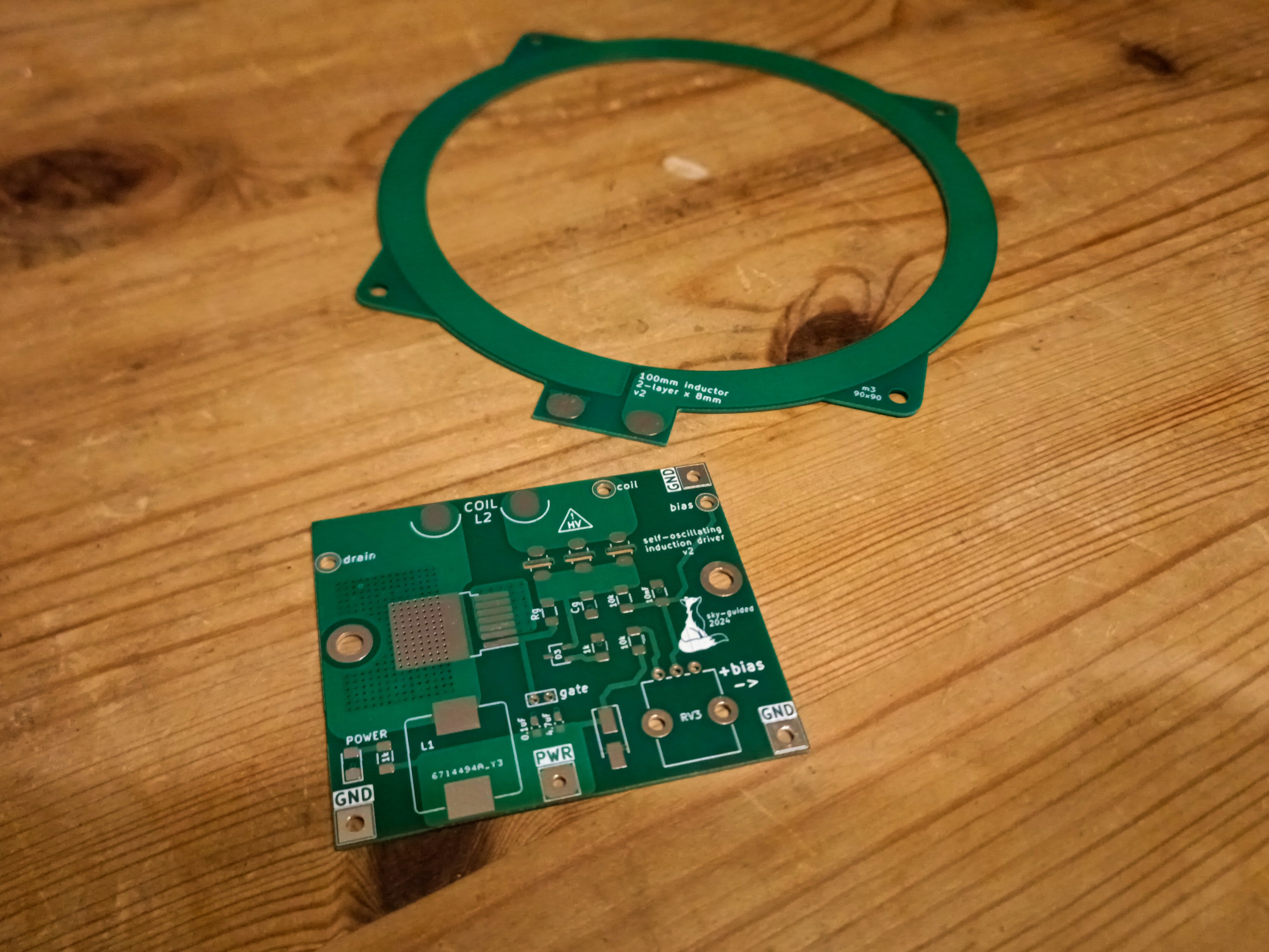

 Collin Matthews
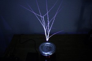
 Zach Armstrong
 CapitanVeshdoki
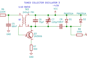
Have you seen the toroid by Humxn
https://youtu.be/YjTv-Hj0h18?si=a5FyBgSM-hgxyPXE