 Petar Crnjak
The often overlooked test jig plays a crucial role in the manufacturing process. My standard practice has become to design a test jig if I believe a product will have sufficient volume or it will be difficult and time-consuming to test manually.
But what is a test jig? It's a mechanical/electronic apparatus that assesses your product at various levels, ensuring the PCB's functionality aligns with design specifications. This is particularly vital when selling PCBs. Testing each one individually can be time-consuming, especially if you need to hook up a lot of components. If this process takes around 20 minutes per PCB, imagine a large batch of 1000 PCBs, it becomes a significant challenge, expense, and liability. However, a well-designed test jig streamlines this process, reducing testing time to a fraction of manual tests. Test jigs come in a variety of options, ranging from inexpensive DIY versions on platforms like Aliexpress to high-end automated solutions. However, designing an effective test jig is a complex task that requires expertise across multiple disciplines. To create a reliable jig, you'll need to design a PCB for a bed of nails, develop a test code, and design a mechanical fixture.
Building a test jig
In this guide, I will not give you some magic files that will give you a working test jig for your PCB, but I will share some knowledge on how to design your test jig and dodge some mistakes and save some money.
Examples will be our test jigs for the PAROL6 robotic arm mainboard and test jigs for the Spectral BLDC motor controller.

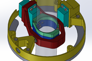
Here we have an example test jig for our PAROL6 robotic arm mainboard! As you can see for the first iteration of the jig you can be creative and see what works and what does not. Later you can use more robust materials and designs.
What test jig need to have?
- bed of nails PCB - usually person who designed a PCB that is being tested will be best suited to design a bed of nails PCB. it is usually identical in size and has holes for nails instead of test pads on the same positions as a PCB we test. bed of nails PCB is used to make contact with your test points on the PCB that you want to test. There are multiple types of pogo pin nails but you will usually use 3 types: needle tor crown type for test pads and cups for thru-hole components.

- clamp mechanism - The clamp mechanism will be used to apply pressure on your PCB so that the bed of nails can make good contact with your PCB.
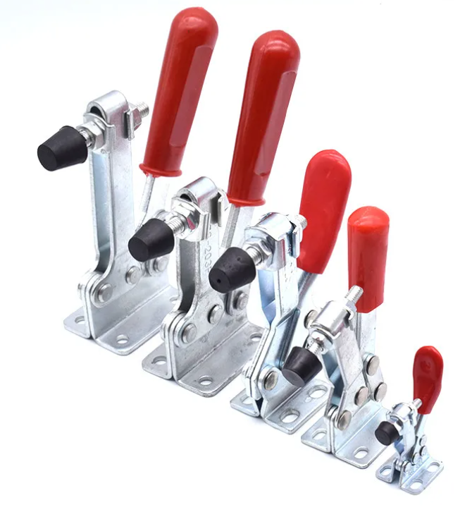
- main body of the jig - usually you can buy these from Aliexpress, build your own or buy expensive of the shelf solutions. Doing one yourself is the best route since you can customize it to your preferences but that requires and advanced knowledge of CAD design.
The main body of the jig will give it a mechanical structure and on top of that you can fit all your wires, and functionalities you want to test inside.
- A computer or microcontroller that runs a testing software.
- Communication or interface devices (Like usb to serial, CAN adapters…) your PC will usually not have a can bus or uart so you will need either and adapter for that or use an Raspberry Pi that has some of these features on its gpio.
- Programming adapters (Stlinks for example)
- A display - not needed but good to have to make debugging and logging process more easier. if test is complex it is recommended to have a display for user interface or to print logs or errors.
- A printer of some kind - not needed but also recommended if you want to produce pass or no pass slips, diagnostics or automatic serial numbers.
- User interface (simple buttons, keyboard or mouse…)
Placing TEST POINTS on PCB we want to test
Designers often rush to include test points without careful consideration. To optimize testing efficiency, think modularly and focus on key testing points based on potential failure and key features that need to be tested. For example, using a test point to measure current or detect voltage if LED...
Read more »
 nicoud jean-daniel

 five above infinity