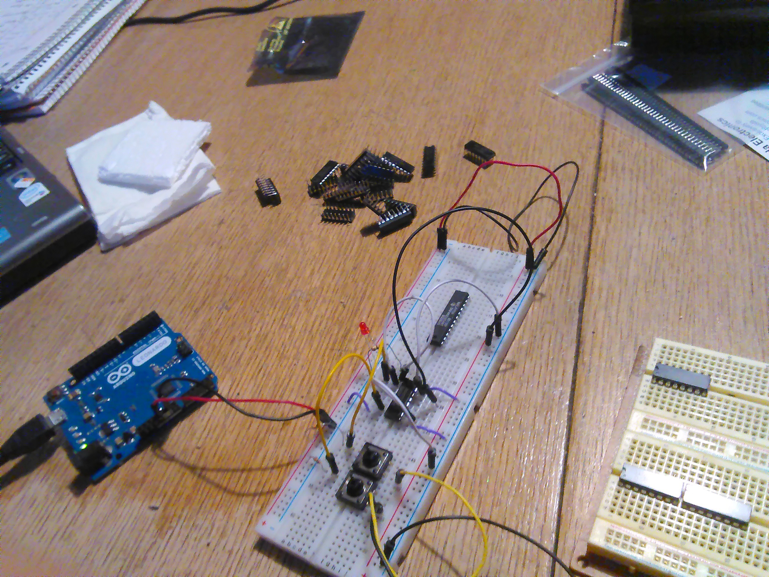
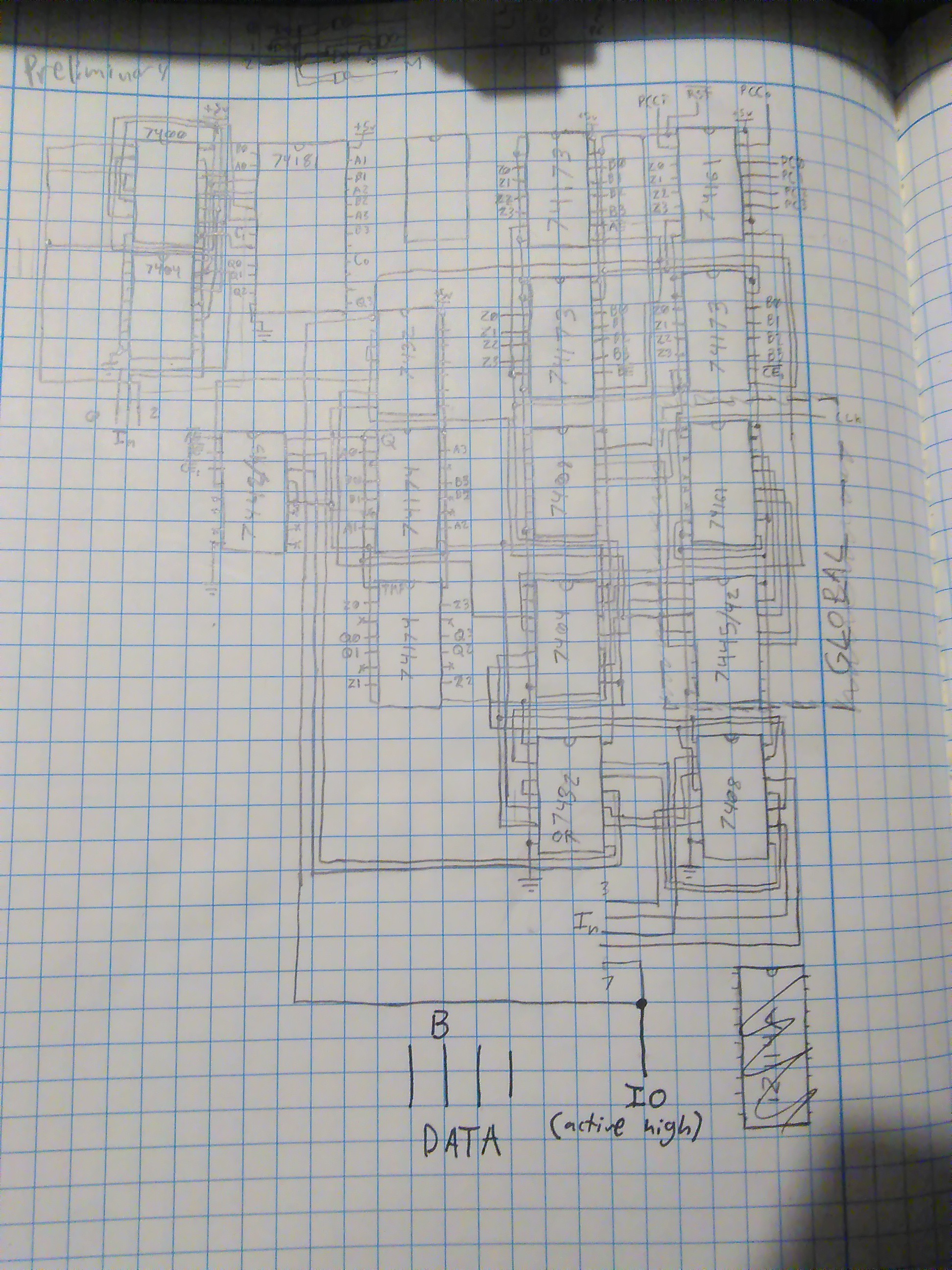
• Got Some 74173 and a schematic, plus a plan

    Dylan Brophy04/14/2017 at 02:50 3 comments

    My 74173s came in the mail today. Tested and working, so I came up now with a plan to make everything and I have a preliminary design. First a picture of my new parts:

    This is basically where I tested and my current setup. Don't worry, I have plenty more breadboards. Anyways, I'll show my preliminary schematic, then my plan for completing this project that would be otherwise a bit too complex for me to handle. My schematic:

    Essentially the slice has 4 registers: A, B, C, and PC. In the instruction they can be disabled, to access IO. The IO address could be formulated from bits 3-6 of the instruction. I still need a way to access IO and registers in the same instruction, and add RAM access. But I want to keep the instruction width 8 bits! I will probably impliment a more complex state machine later. Also, take note of the logic that processes the first 3 bits of the instruction. Kudos to @agb.cooper for coming up with that logic. See his project #The 74LS181 ALU for a better schematic. It's basically to lessen the # of bits needed in the instruction. The idea is to remove ALU functions you don't need in exchange for more instruction bits (At least in my case). So yes, lots to improve.

    My plan is to make the Slice in sections on breadboards to make sure everything works, then as each part is finalized solder it onto the PCB. I'll start with a registers section. What other sections should I break it up into? ALU, random logic...? We shall see!