 Paul Andrews
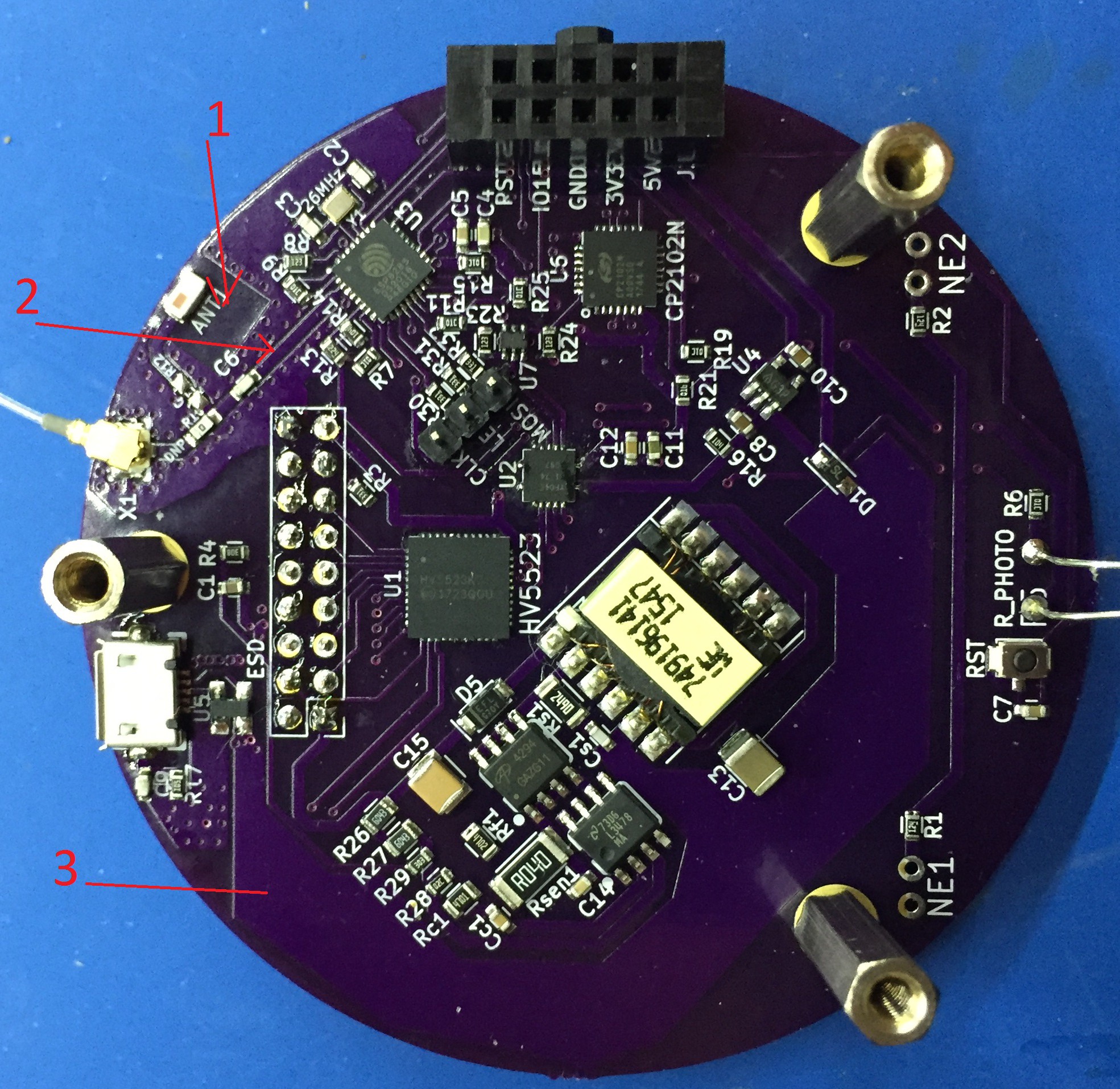
Features include:
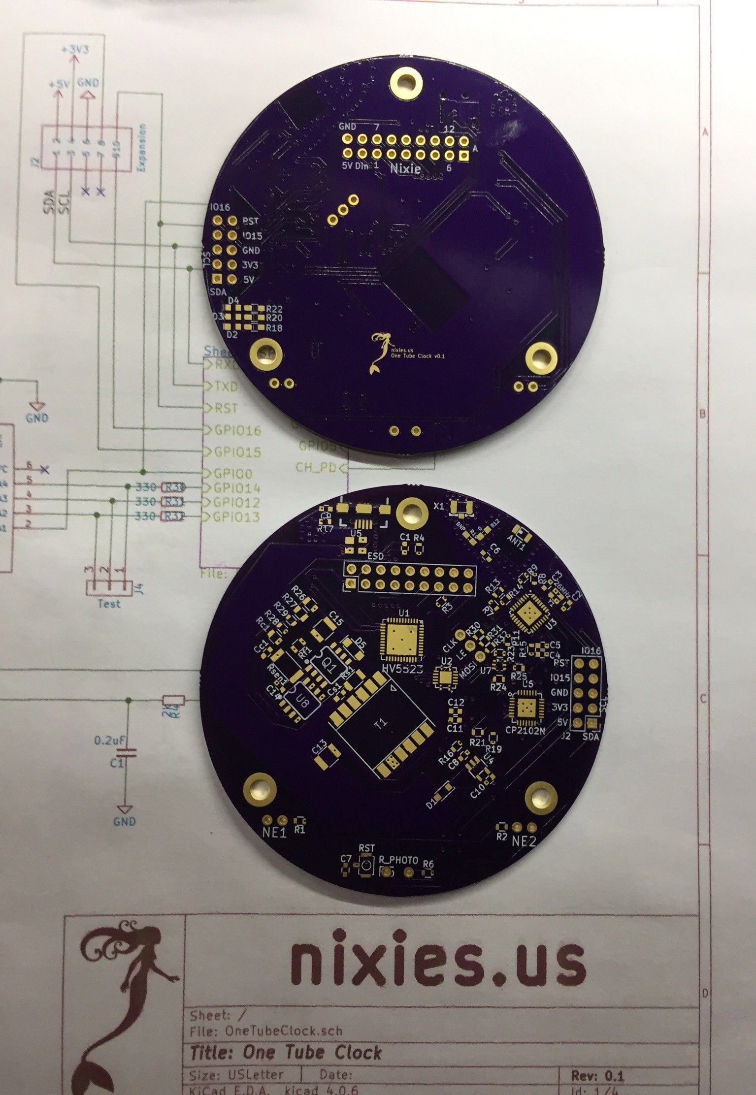
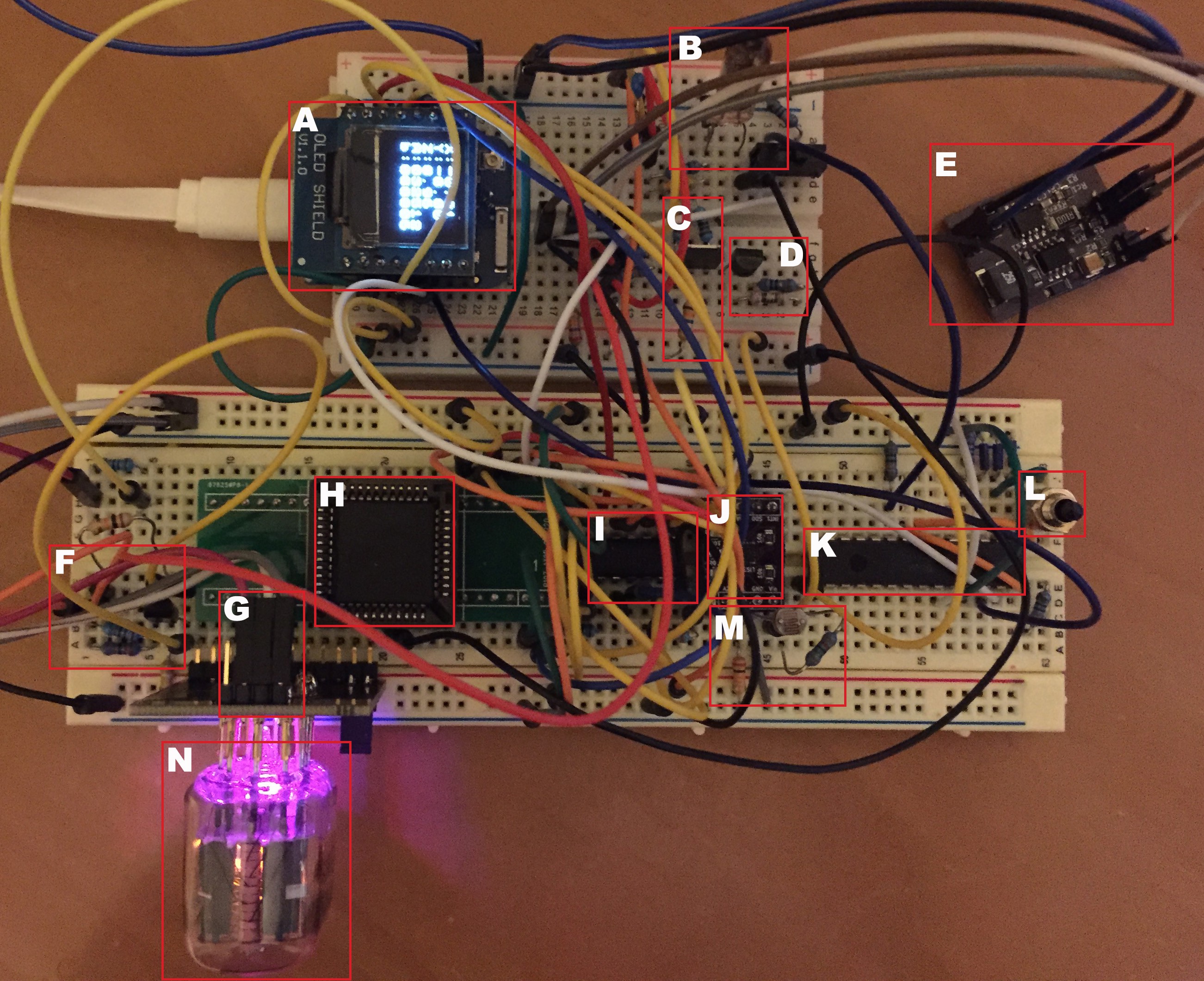
- Board is on OSHPark
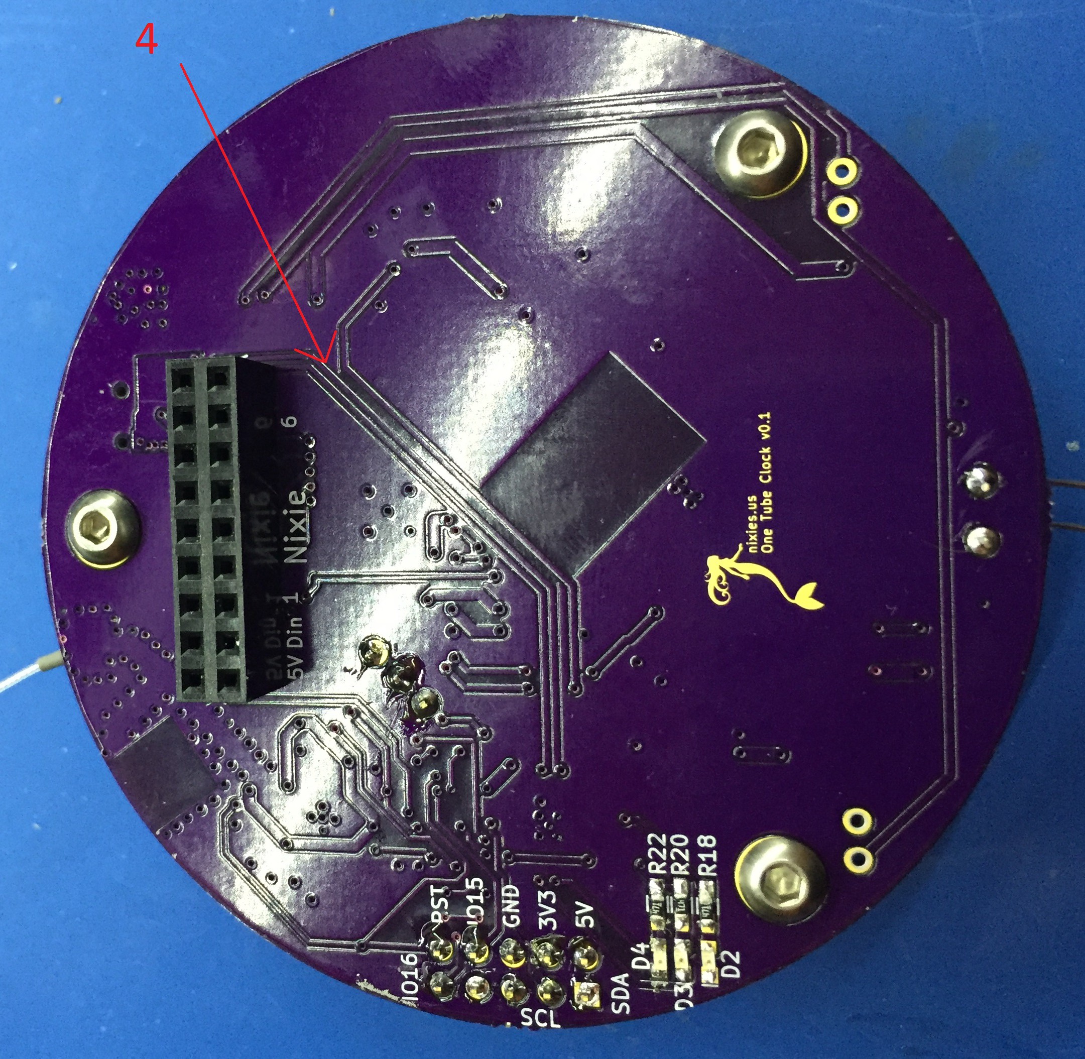
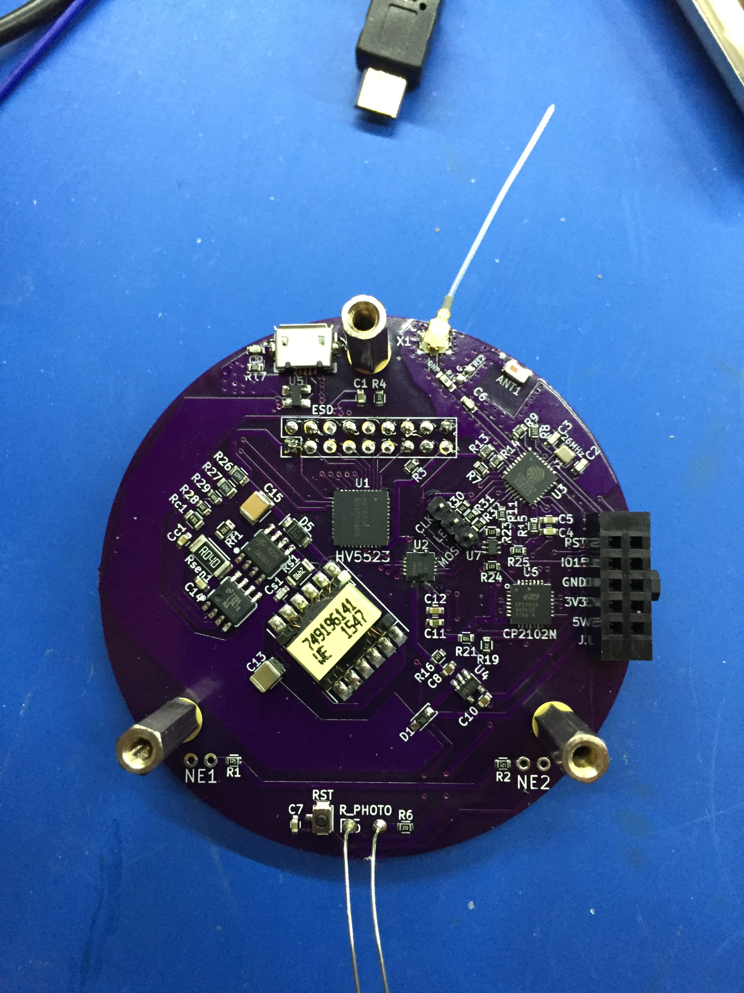
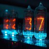
- Any Nixie tube can be driven using an adapter. There are several on OSHPark now: IN-12, B5991, CD25, CD43, ZM1100 etc., IN-18, NL840, NL807, NL5440, NL5440A, NL5441, NL5441A, B54370A, B5440, B5440A, B5441, B5441A, GR10J, GN-6A, GN-13A, XN-3, XN-13, etc, ZM1020, HB-106, B6844A, B6091, B5092, GN3, GN4, etc,
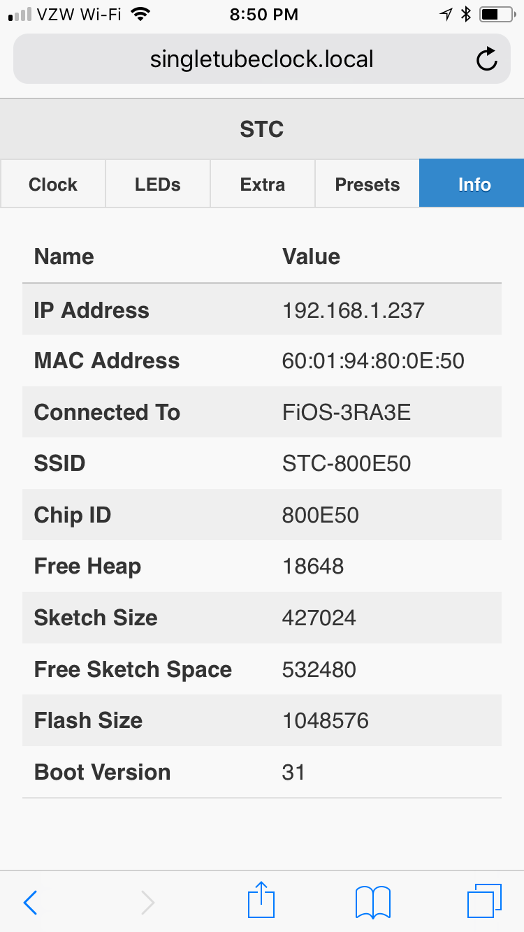
- It is driven by an ESP8285, so it has built-in WiFi.
- It is powered from a USB port.
- KiCAD project is on GitHub
- It can be programmed through the USB - source code is available on GitHub.
- It has an I2C expansion port, so you can add other sensors and outputs such as buttons, motion sensors, displays, and RTC(!) etc.
- It has a light sensor for auto-dimming.
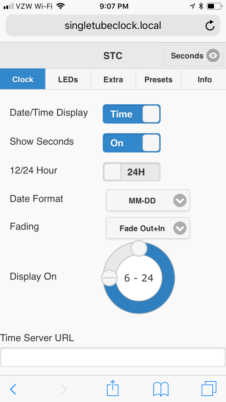
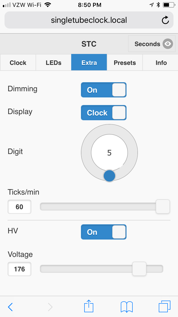
- The default application:
- Synchronizes the time with the internet
- Presents a web configuration GUI
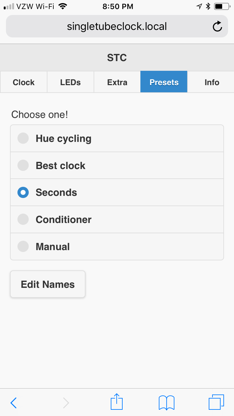
- Has five presets for easy switching between different configuraions
- Has a blanking period
- Can drive a tube either as a clock, or a counter
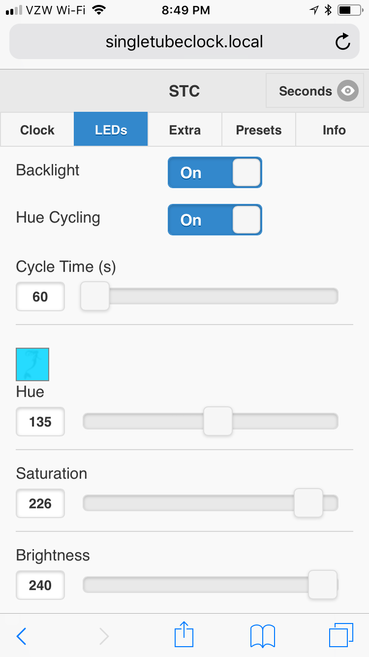
- HV can be modified from the GUI to increase the current through the tube. This means the device can double as a cathode de-poisoner.
- You can control the backlighting

 John Lonergan
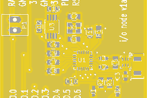
 Justin
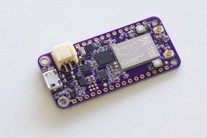
 Jared
Jared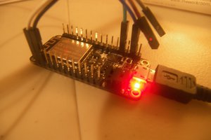
 Alexander
very nice, I thought about using the esp8266 on mine but was space constrained. if you look at my mini clock I have a circuit on there that might interest you. the charging / super cap circuit. also runs off Lipo.