I loved electronics as a kid before other priorities took over. Then one day on a training ride my GPS battery died and I credit that moment with getting me back into electronics. That was some years ago and looking back the design is primitive and probably shows where I left off as a kid.
Nonetheless I use it to this day and it has never let me down. It's performed in all kinds of climates from freezing to 100+F with sustained speeds in the mountains of 40+mph. So I figure it's worth sharing.
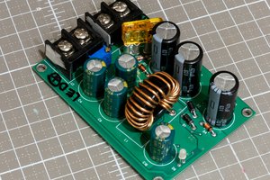
The TRIPLE5dps is a SMPS designed for bicycle hub dynamos such as the Schmidt SON or Shimano Alfine. It was my first serious work in many years and is a discrete component design using three (yes 3) 555 timers.
Specs:
- Weight: ~150g
- Size: 10.3cm (L) x 4.6cm (W) x 3.2cm (H) using Polycase ID-1741 case
- Operating speeds*: 8-70mph (10-112kph)
- Input: 12-150VAC (P-P), 12-30VDC, 600mA max
- Output: 5VDC, 1A / 5W (Based on Shimano Alfine dynohub with 700c wheel. Different speed limits may apply depending on the dynohub and wheel size combination)
- Internal fuse protection
- Over current & volt protected
- Efficiency: 75% average
Note: the zip file in the files section contains the Eagle schematic, board, and parts library along with the parts list in Excel.
CIRCUIT DESIGN
The TRIPLE5dps gets its name from the use of three 555 timers to perform the PWM, duty cycle control, and limit functions. It is truly amazing that in our culture of disposable technology the 555 timer is still in mass production forty plus years after its debut.
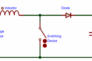
The TRIPLE5dps is a fixed frequency PWM running at 100KHz, utilizes a buck topology, and delivers 5VDC within -3%, +0% with less than 50mV ripple up to 1A. Included features are input over-current protection, output over-volt protection, and output current limiting.
DESCRIPTION OF OPERATION
The dynohub’s AC input is connected to the rectifier section through two fuses. F1 is a slow blow 1A fuse and protects against an internal failure and is used to allow for in-rush current to charge C1 that will occur when connecting to a DC power source such as an automotive power outlet. Do not connect to utility AC! F2 is a thermal fuse bonded to the heat sink tab of Q1 and disconnects the AC input via heating from Q1 when an over-volt condition develops on the output. Diodes D1-4 form a full wave bridge rectifier with filtering capacitor C1 to provide the working DC buss voltage used by the power supply.
Transistors Q5, 6, and 8, along with R4, R6, R7, C3 & C4, and D6 form a simple linear regulator that is used to power the control circuits. It provides a regulated 12VDC and 10mA of current. Because the control circuitry only requires a working average of 7mA, pass transistor Q8 can tolerate the voltage stress without excessive dissipation. This design keeps allows the use of a cheap off-the-shelf choke by eliminating the need for a secondary winding & associated circuitry.
The PWM core is comprised of three 555 timers. Two are housed in the 556 package (timer #s 1 & 2), and the third (#3) is a stand-alone 555. All three are the TLC CMOS variant to reduce power consumption and improve switching performance. The PWM is divided into three operating sections: ramp generator, duty cycle control, and PWM.
Timer #1, Q9, Q10, R9, and C6 generate a linear ramp timing signal used by other sections of the PWM. Q9, Q10, and R9 form a constant current source and together with C6 set the ramp frequency. The ramp signal is used by timer #2 along with R21 to establish duty cycle limit timing (~50%). The square wave output of timer #2 drives the reset pin of the PWM (timer #3) low when the duty cycle limit is reached which turns the PWM output off. The duty cycle value is set based on the maximum output load of 1A at...
Read more »
 Kevin LO
 w_k_fay