Stefan Lochbrunner
-
@SUFs audio breakouts
07/16/2015 at 17:01 • 0 comments@SUF was so kind as to send me some breadboard compatible modules he designed but since he's quite occupied with his other projects I am writing the logs about them. The files have been merged into the existing repo but you can also find the original files here.
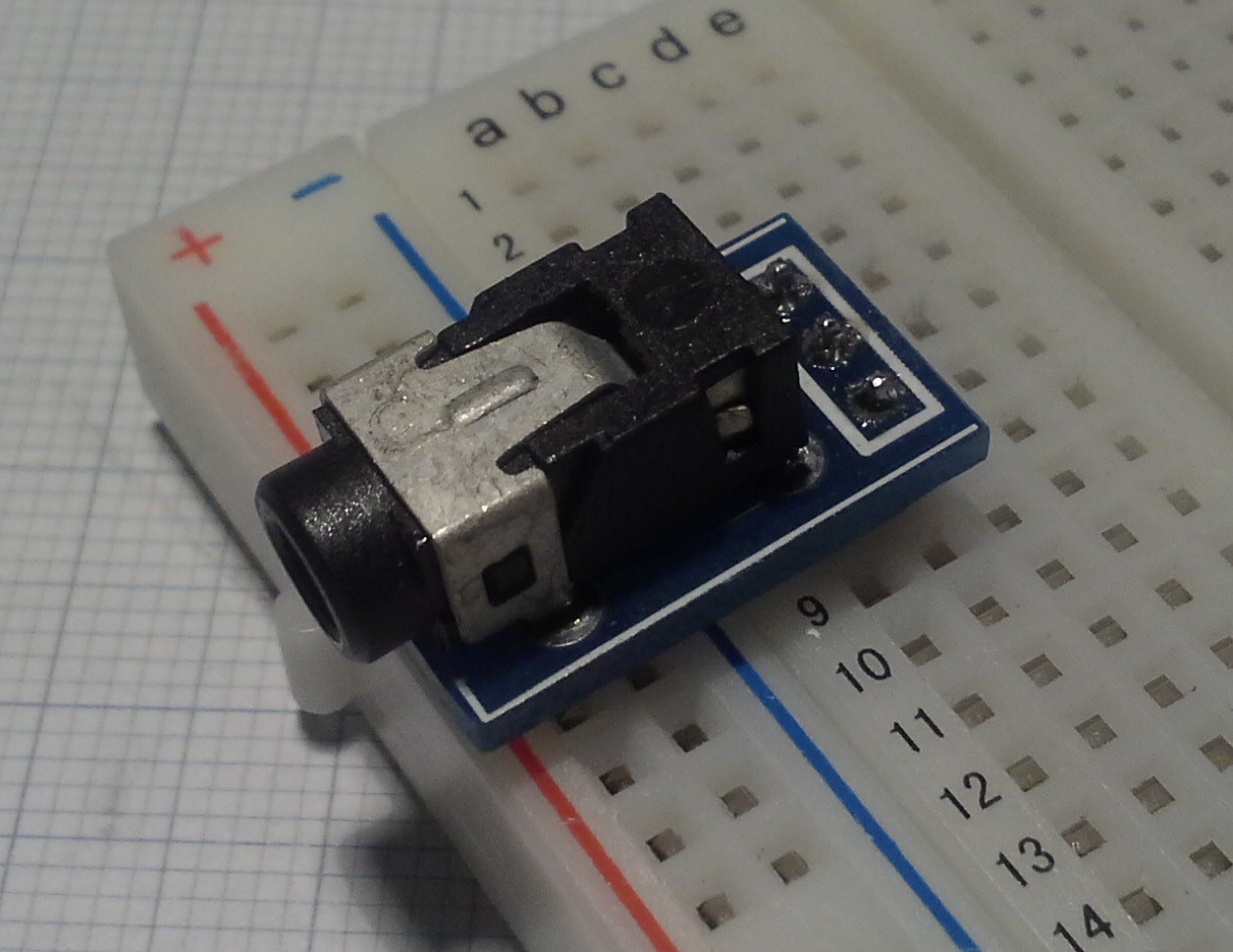
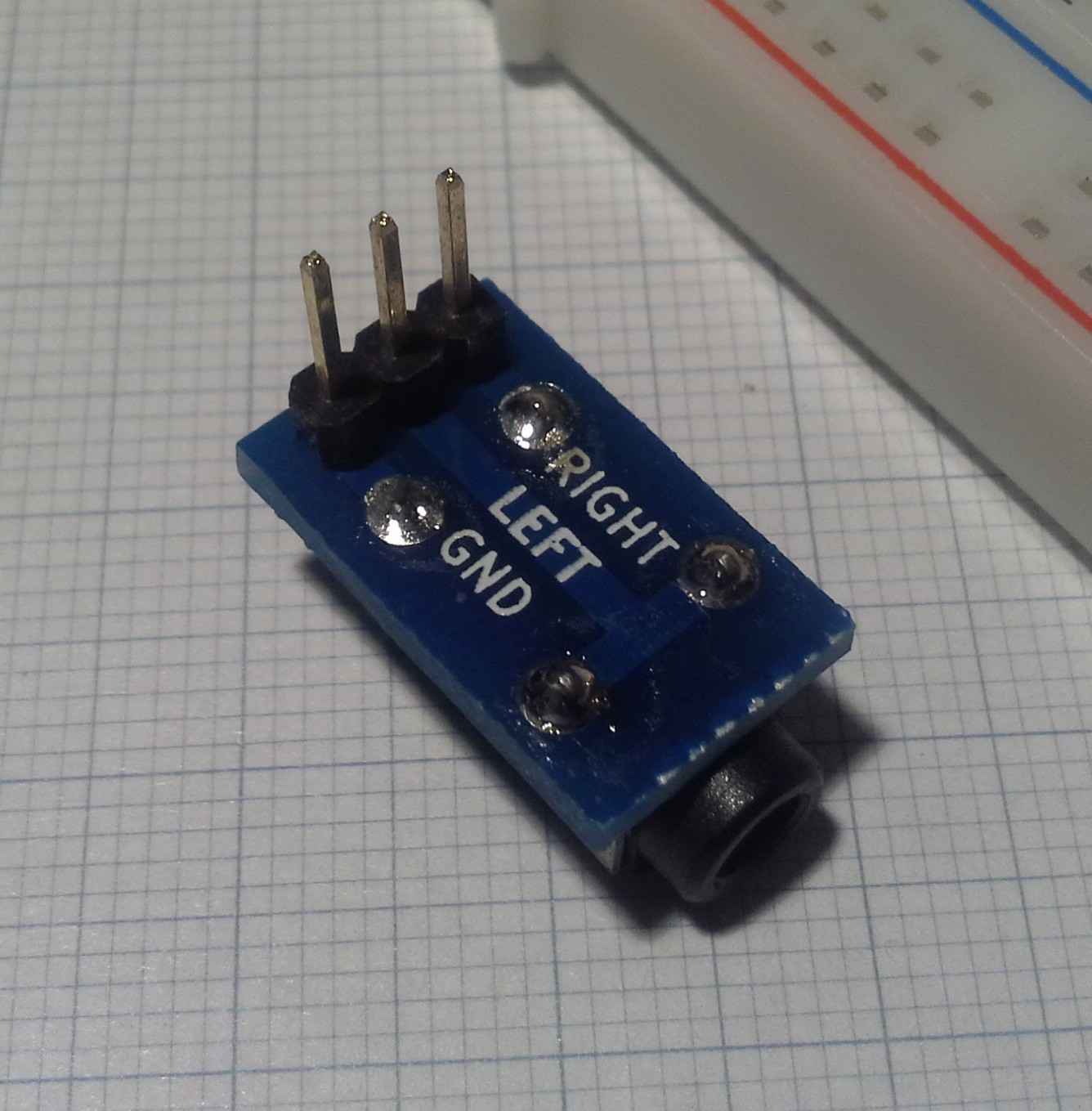
The first of the two modules is a for 3.5mm TRS jack breakout:
![]()
![]()
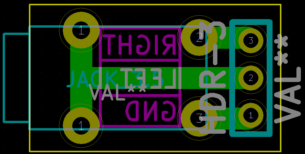
It's a straight forward breakout so schematics shouldn't be necessary but the board files are in the repo and look like this:
![]()
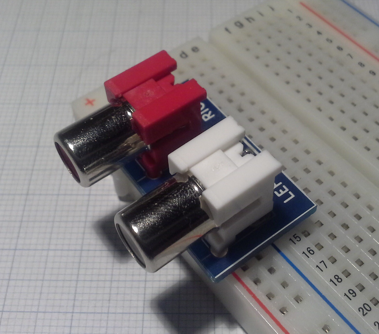
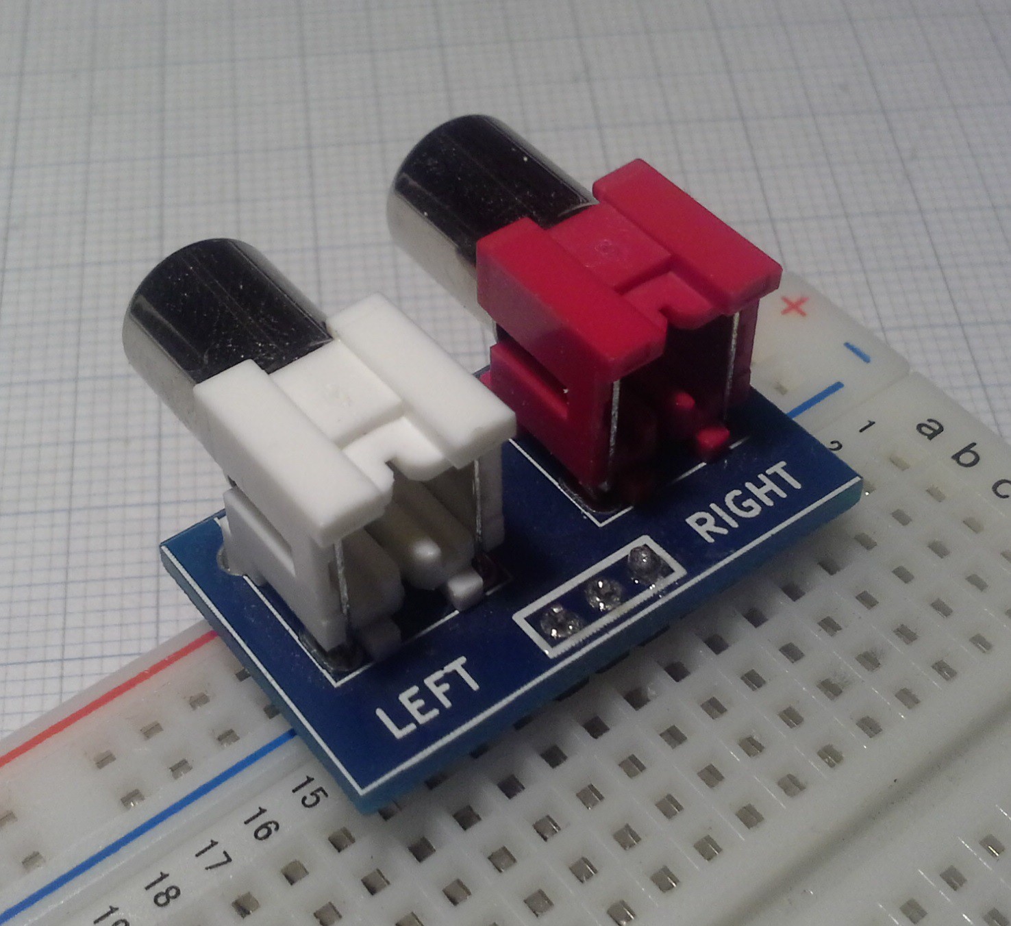
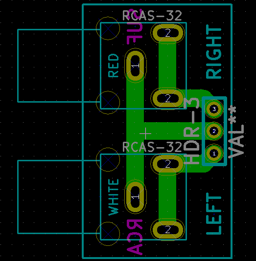
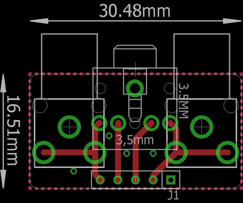
The second board is a stereo RCA jack breakout:
![]()
![]()
Again, schematic is self explanatory. Board looks like this:
![]()
Despite this log being called audio breakouts, you could of course also use this board for composite video.
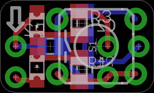
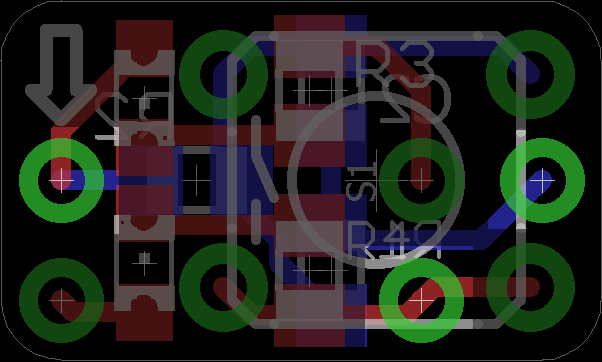
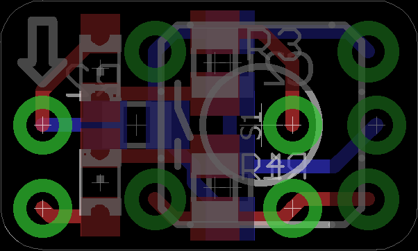
Since both of these boards do the same thing and to maximize the number of different boards that will fit on a panel, I combined them into a single board:
![]()
The reason for the changed footprints is that these seemed to be more widely available (e.g. from Adafruit or off of eBay). I also broke out the sense (?) pins that let you detect if something is plugged in, cause why not. This seems to also be possible for the RCA jacks which I will add in the next version.
-
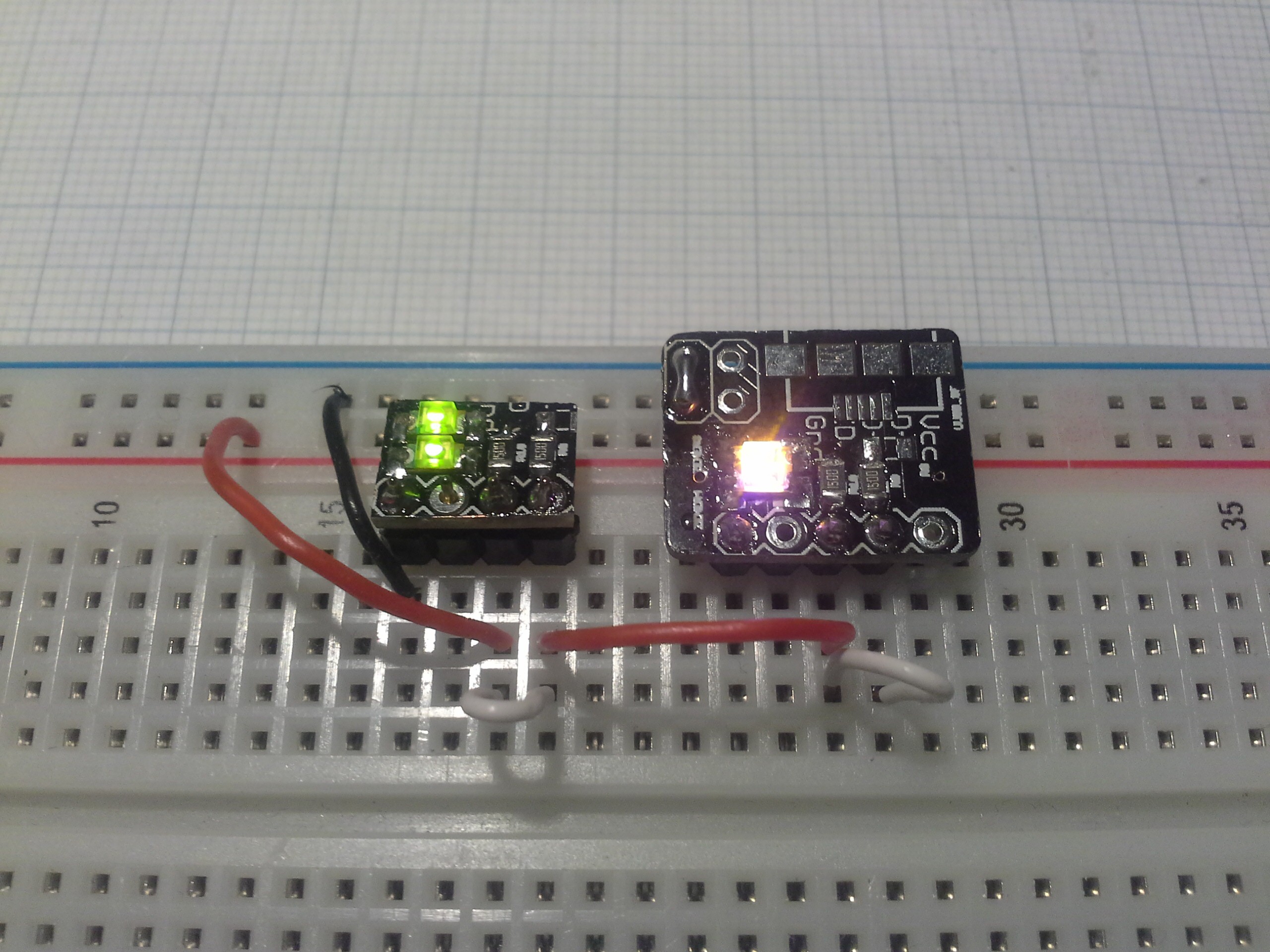
SMD LED breakout
07/06/2015 at 13:43 • 0 commentsModification of the button board.
![]()
![]()
If there's something I dislike as much as hooking up a button with pull resistor, it's hooking up a LED. Yeah, I'm that lazy. Fortunately, the LEDs I have been using for quick tests didn't burn when I put 5V across them without current limiting resistors (they may or may not have turned from green to yellow though...).
Anyway, the other day I was thinking about putting together a new board but then I remembered the unused space/layer on the button w/ pull-up/down board. The reason why I wanted to combine the two is that when I order the PCBs and get ten panels I probably won't ever use ten buttons. This way I can at least use some of the boards for LEDs (and save the other LEDs from being tortured).
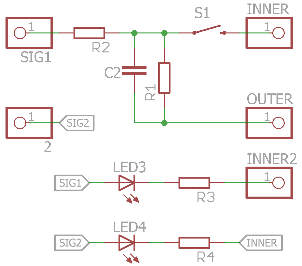
The way the button works is just like the previous version with the addition of an arrow indicating if the resistor pull is up or down. To make it a little more apparent how it works I've highlighted the pins that need to be populated for this mode:
![]()
The two pins on the right plug into the power rails and since they're staggered the board could also be used in the center of a breadboard. (Sorry for using these round pin header footprints that look just like the through holes of the tact switch but these fit best into the corners of the board)
To use the board for LEDs, a different configuration of pins is required:
Once the LEDs are soldered in place they can still be used independently or both in common anode cathode configuration. I imagine the latter being done by plugging the boards into the rails. I barely use LEDs in common anode config so I might as well have tied the cathodes together but I like having options.![]()
Update:
Here's just a quick hack on how to turn the µUSB Breakout into a breakout for SMD LEDs:
![]()
![]()
Update 2015-10-05
Here's just a quick demonstration of both modes of the board:
The LEDs are hooked up such that only one lights up in either state of the button. In the unpressed state the pull-up resistor is in series with the bottom LED resulting in a lower current and therefore brightness.![]()
-
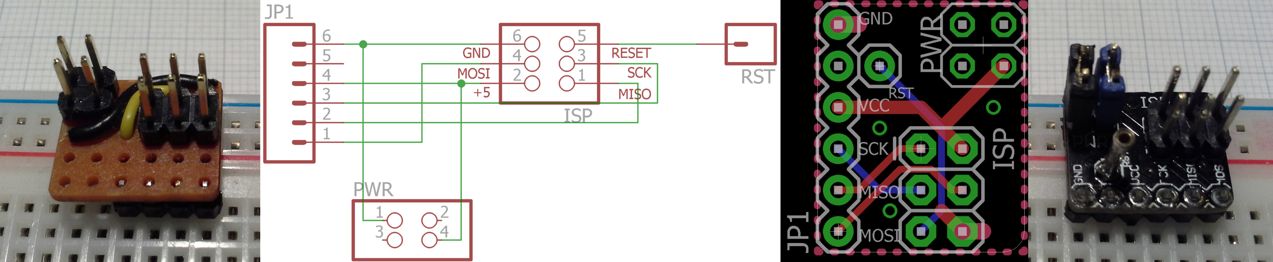
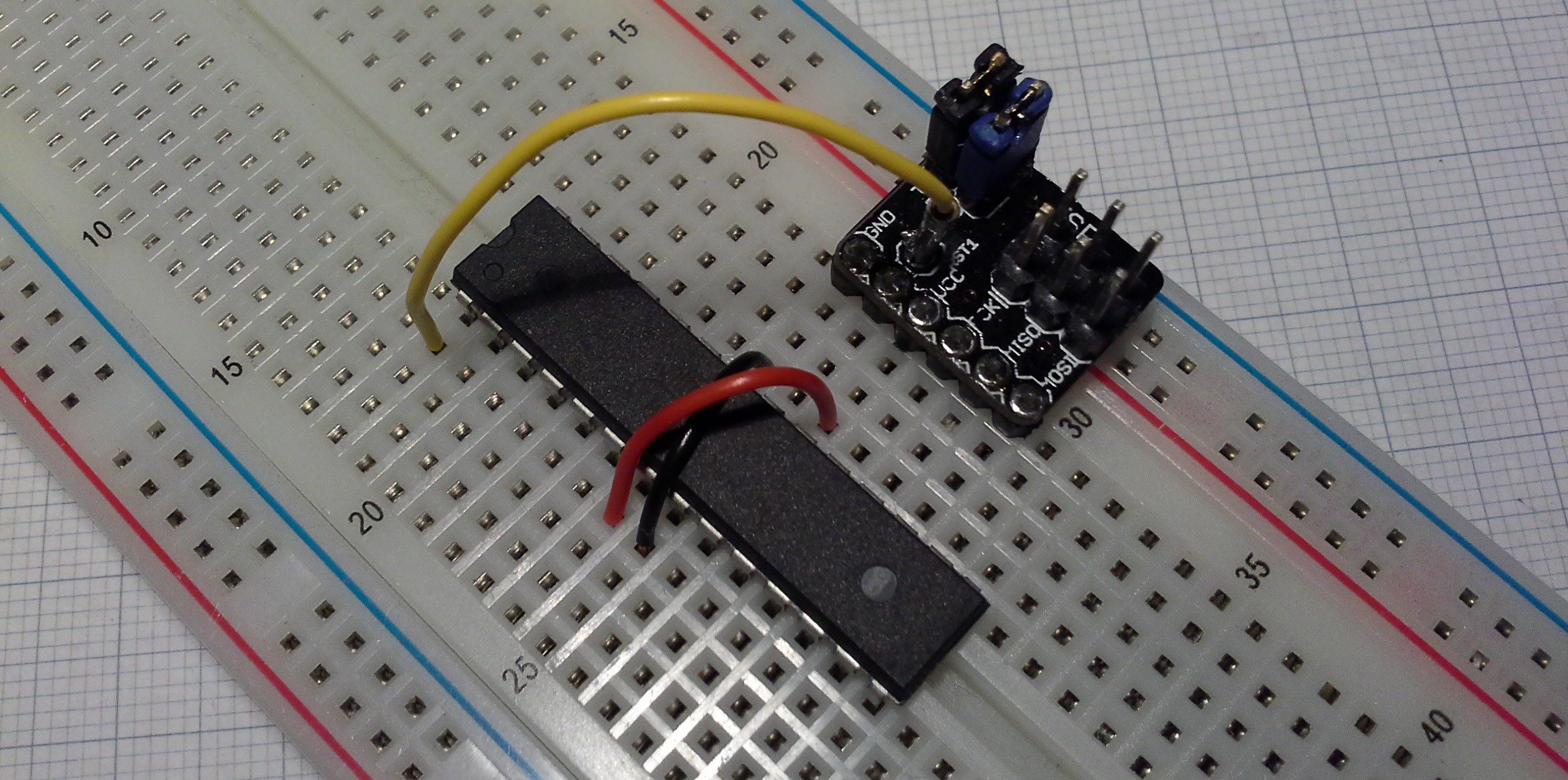
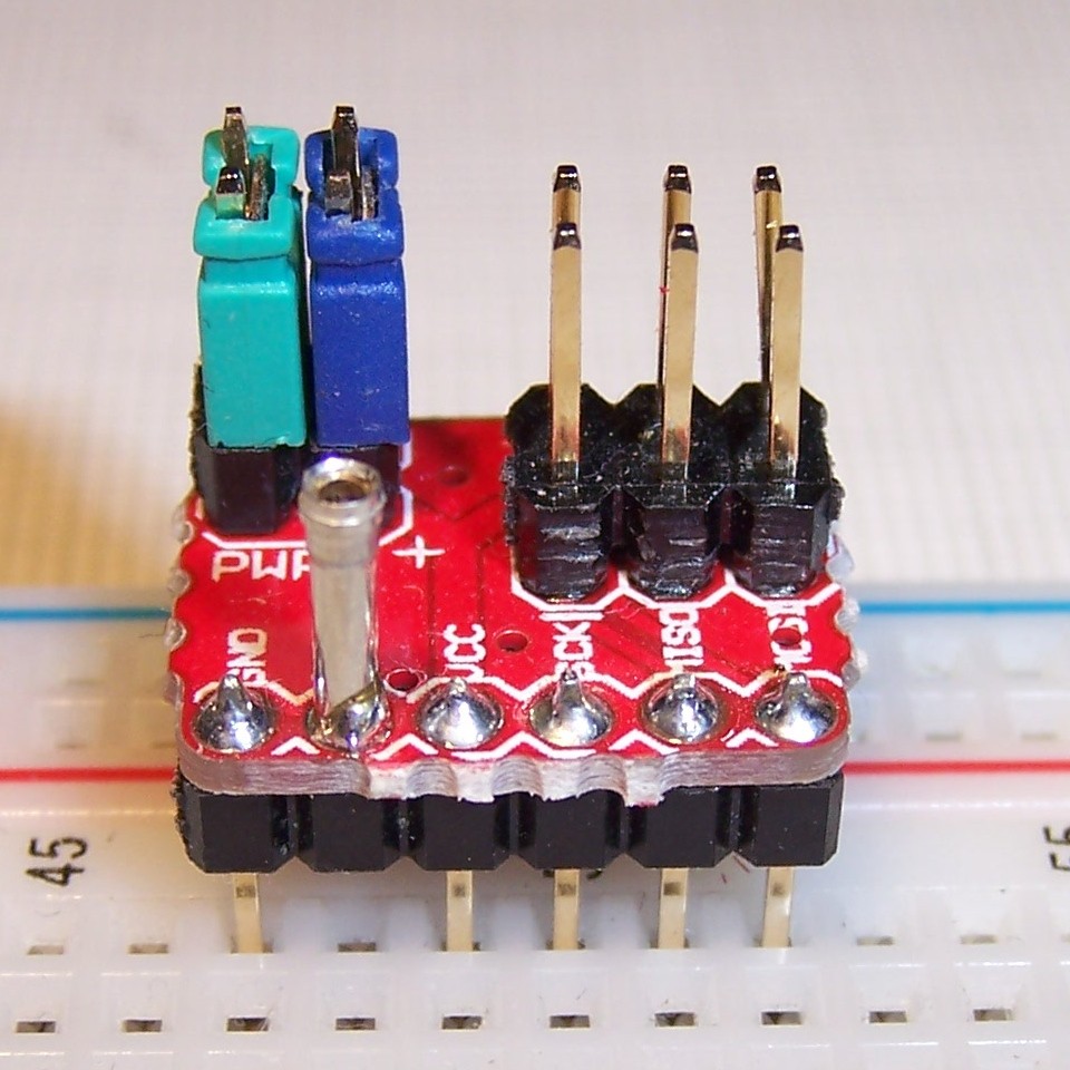
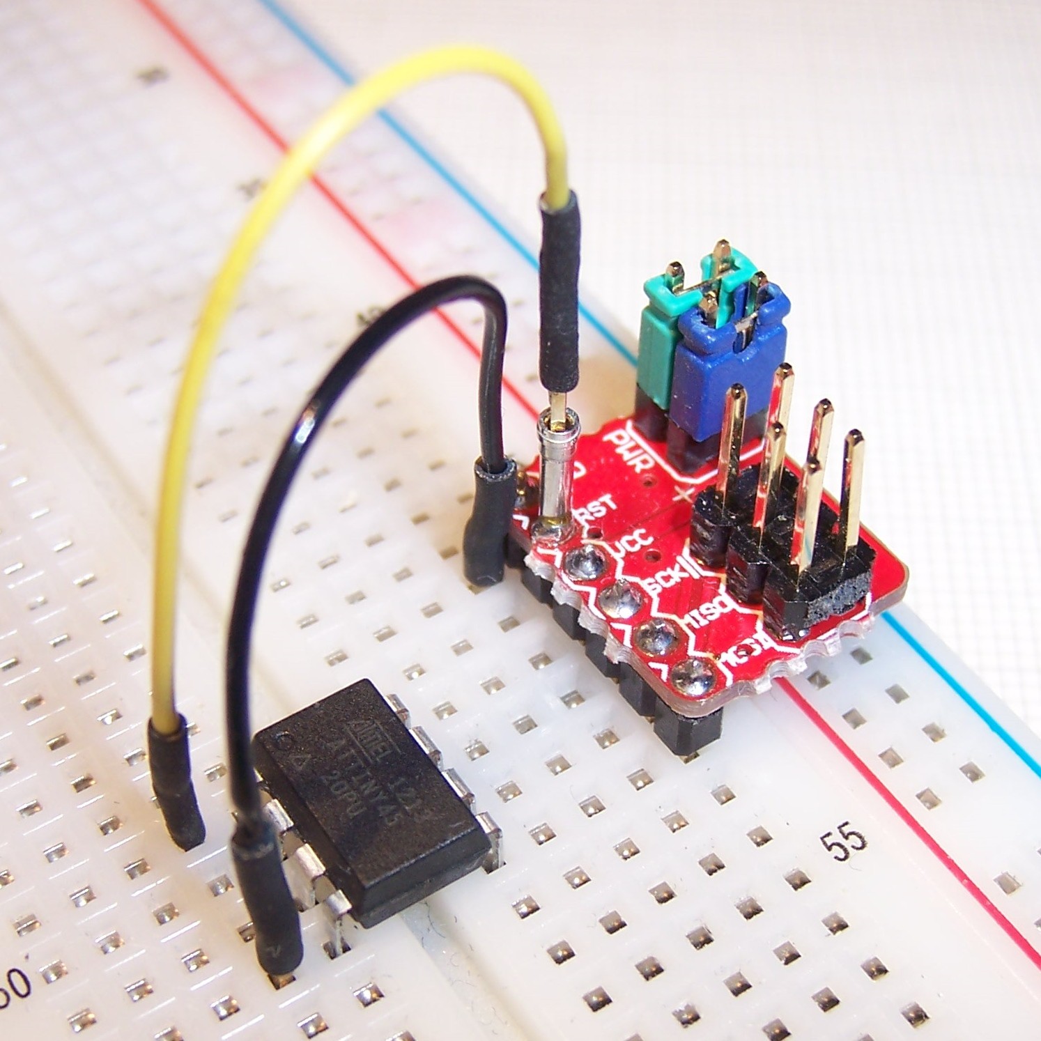
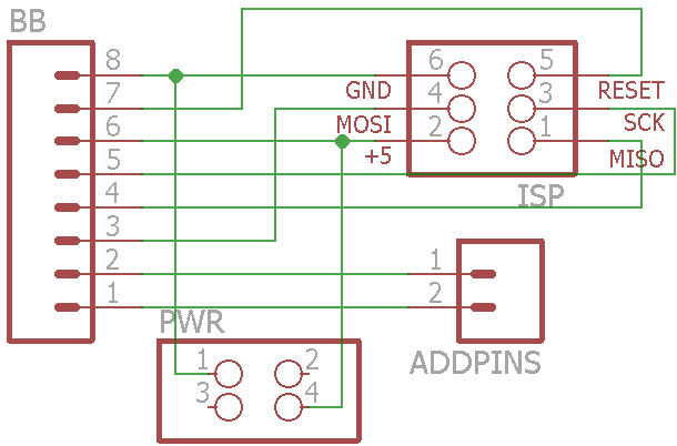
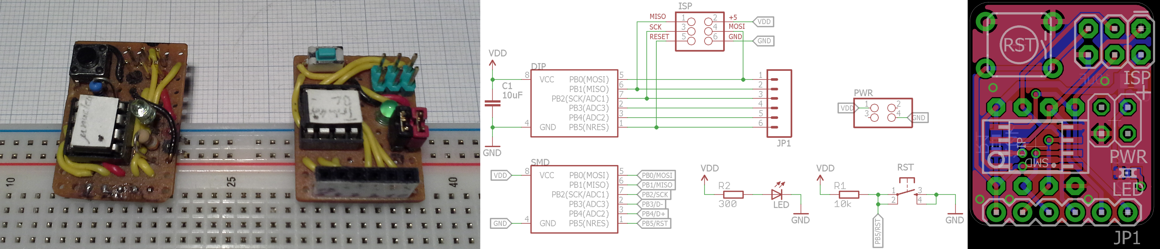
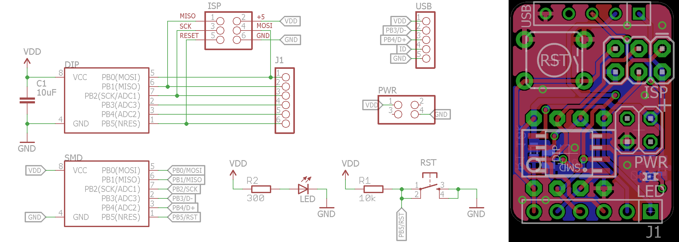
ISP breakout
06/17/2015 at 19:13 • 0 commentsFor completeness here's a log for the ISP breakout and the link to GitHub.
![]()
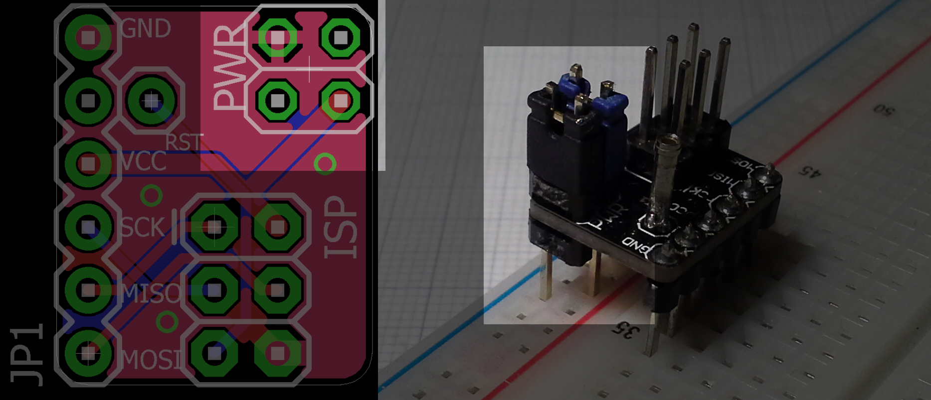
It's pretty straight forward so I won't go into details but it's handy to have (especially if the pins are labeled). The only gimmick is that the pins are in the same order as an ATmega328 (and ATtiny45/85) making it easy to set it up for programming:
![]()
Obviously a jumper wire is required for the reset signal (and GND on ATtiny, see below). The pin next to the reset socket (between GND and VCC) is not connected to anything and might as well be left out.
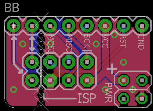
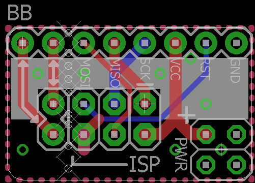
Update 2015-11-05:
This update on v1.1 (which is the version on the current panel) of this breakout has been long overdue so here it is:
Besides minor rerouting the only major change is the move of the RST pin which is now part of the 1x6 header and should be assembled like this:
![]()
To maintain compatibility with the ATmega328 instead of a pin a single female header should be placed in this location.
And here's just a quick example of the compatibility with an ATtiny45 mentioned above:
![]()
Update 2015-11-15:
I made a small modification to allow the board to be used as an adapter for devices with a 2x4 header (e.g. an ESP-01). In this case the pin order on the 1x8 header is pretty messy but I found myself needing such a board a couple of times. If you just want the ISP breakout the part with the additional pins should break off easily.
![]()
![]()
Update 2016-01-24:
Just another even smaller modification. I was thinking I could show the pinout of the 2x4 header on the bottom silkscreen but then the question was if I should use the numbers of the pins and indicate pin 1 on the 2x4 header (like the MISO pin is indicated on the ISP part of the header) or make it specific to the ESP-01. Because I'd like to use this as a general purpose adapter using the ESP pin functions wouldn't be very useful and since the pins are not in a coherent order numbers wouldn't be very helpful either. So this is what I ended up doing:
![]()
A large white area on which one can write the pinout of what the adapter is intended for or make some color coded markings.
-
"PWR thingy"
06/16/2015 at 22:14 • 0 commentsThe project that led to this was the first version of the ATtiny prog board which was inspired by the Digispark. It was around the time of the Kickstarter where I saw it being plugged into a breadboard and its power rails. Since that's a quite smart idea I built the prog board to do the same in order to decrease its width. However, this has the downside that the board can only be used on one side of the breadboard (which is only a slight inconvenience but if it can be avoided it helps to reduce the mess of wires on my bench/desk).
Until recently I haven't seen this being done anywhere else. Most of these boards are in a DIL configuration that requires more space on a breadboard (granted, two pins don't weigh in that much on larger packages but I think they do in this case).
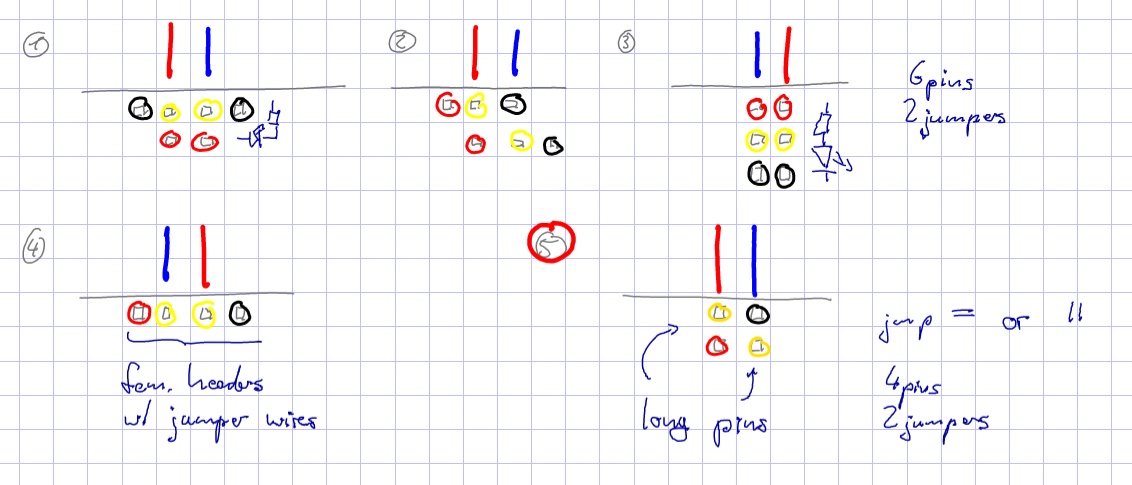
Anyway, to circumvent the problem and make the prog board usable on both sides of a breadboard I threw around some ideas:
I settled on the 5th version and the way it works is the following: There's a 2x2 header on top of the board but two diagonally opposed pins are longer and reach into the power rails. These two long pins are only connected to the circuit via two jumpers. In the above sketch placing the jumpers vertically would connect the supply voltage of the board (red, bottom left pin) to the long pin plugging into the positive rail (red line, top left pin) and the other pins are connected similarly.![inception of the PWR thingy]()
If you now place this assembly on the other side of a breadboad, where the rails are inverted, all you have to do is connect the jumpers horizontally. To illustrate this better here's the board layout and picture of an ISP breakout that uses this system:
![PWR thingy]()
As you might have seen, I use this on most of these widgets. It solves a problem but also creates a new one if you forget to place the jumpers correctly. Therefore I've been thinking about some sort of rectification attachment to replace the jumpers, though I'm worried that an off-the-shelf rectifier would have a too high voltage drop. But then again, if I was using such a rectifier, I might as well put it on the board and omit the PWR thingy.
Edit: I added a '+' to the silk screen to indicate the Vcc pin which should make setting the jumpers easier. (I didn't bother updating all the images for such a minor change but I'll put some here)
-
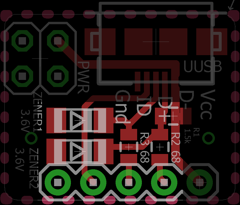
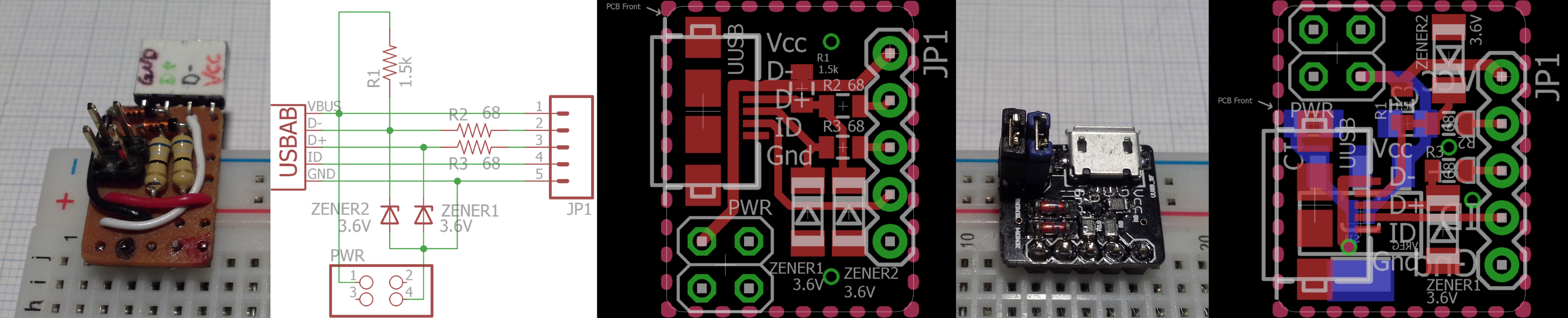
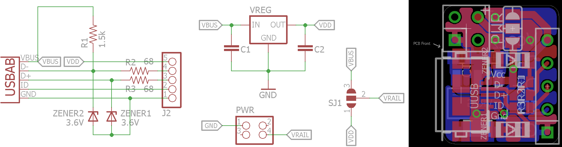
µUSB Breakout
06/16/2015 at 16:56 • 0 comments![Evolution of the uUSB breakout]()
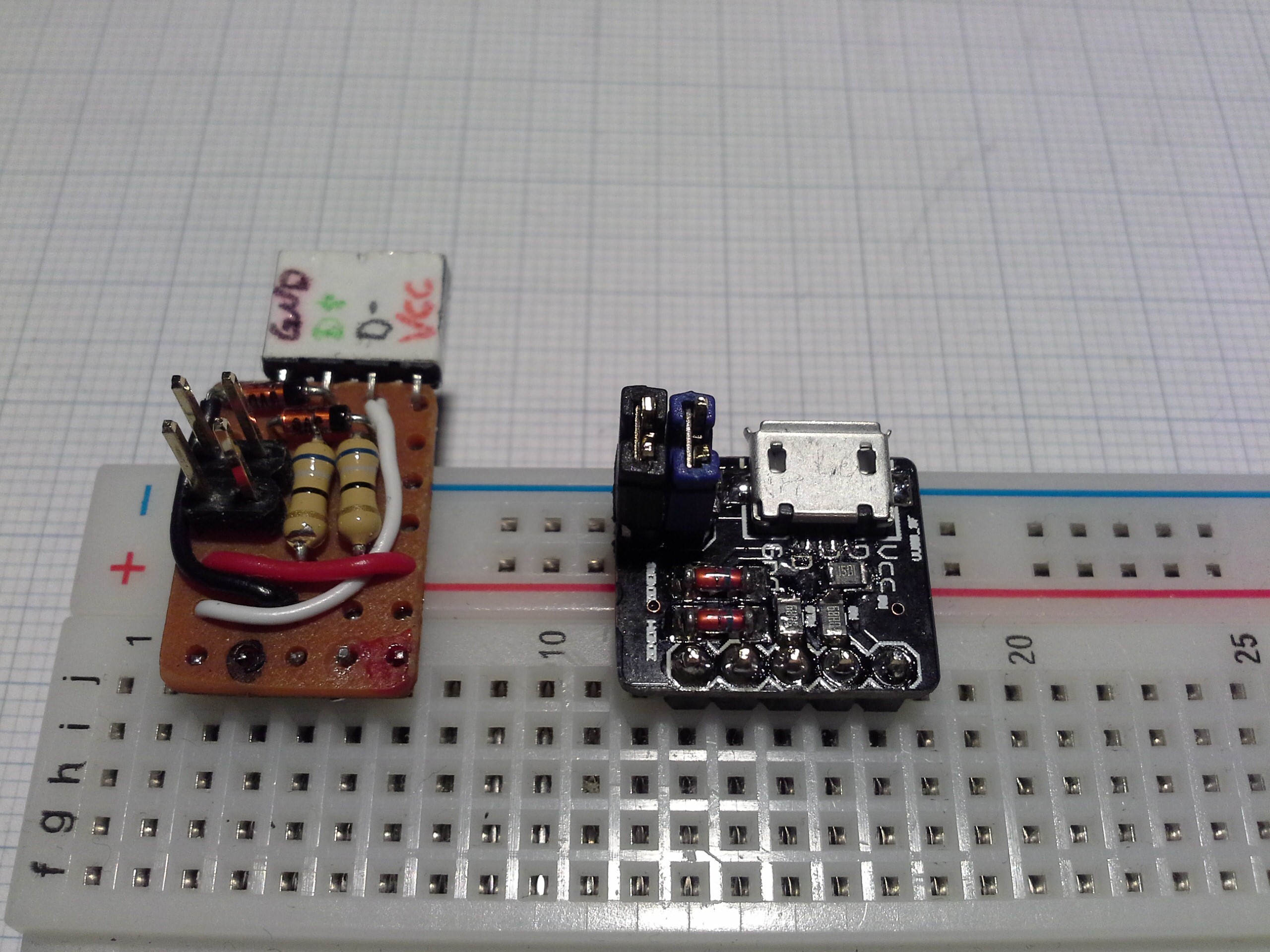
As you might guess I got tired of putting together the "VUSB circuitry" so I put it on perfboard. I briefly mentioned the prototype it in #Pro Trinket USB Keyboard in this log.
I didn't quite like the female headers and matching USB cable so when I had some space on a PCB order I designed a better board for it.
![]()
Once I had this nicer version of the "VUSB circuit" board there wasn't really a point in keeping all the other duplicates of the board except that it's easy to modify into a generic breakout: just short the pads of the 68Ω resistors and leave the other pads unpopulated.
It can also double as a simple breadboard power supply by feeding the power rails via the PWR thingy. Since the complete bottom layer was unused in v1 I elaborated on the idea of using it as power supply by putting footprints for a voltage regulator on the bottom in v2.
Update:
![uUSB breakout v3]()
Added v3 with minor redesign to supersede v2. Now it can act as a power supply with the following modes:
- Supply rail and Vcc pin (called VDD in schematic, labeled Vcc on board... sry) with 5V directly from USB (regulator not populated, short all 3 pads of solder jumper)
- Supply regulator with 5V from USB which in turn supplies rail and Vcc pin (short center and top pads [boad view]/Vrail and Vdd pads [schematic])
- Supply regulator from rail and get regulated voltage on Vcc pin (short center and bottom pad/Vrail and Vbus pads)
I'm not sure how useful the last mode is going to be, considering the size of the board and redundant pins.
-
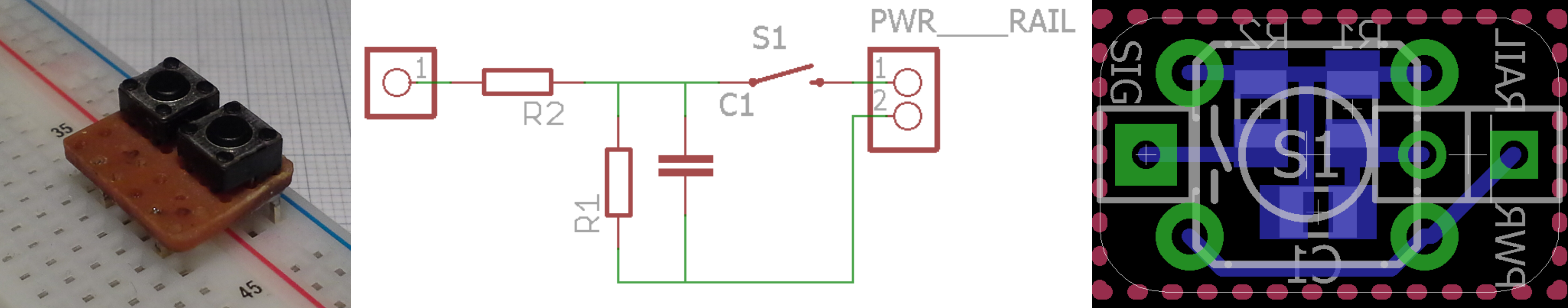
Button w/ pull-up/down
06/16/2015 at 16:54 • 0 commentsGitHub for schematics & board files.
![Evolution of the button with pull resistor]()
This one is so simple that I don't know why I even bother...
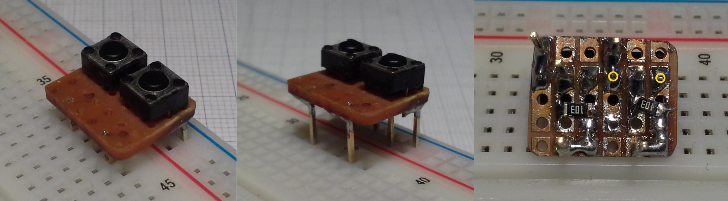
Anyway, here are a few views of the prototype:
![]()
It plugs into both supply rails and in the bottom view you can see that the output is pulled to whatever the inner rail is. For clarity I've marked the two pins of the tact switch, which when pressed connects the output to the outer rail. Therefore, depending on which side of a breadboard the buttons are placed, they either act as pull-down (left) or pull-up (right).
When I drew the schematic and board of the remake I was unsatisfied with the utilization of board space, which is why I added footprints for an optional low-pass filter. Though there's no footprint for SMD tact switches it should be possible to solder these to the through holes as well. I would have liked to also accommodate 3mm wide switches but I haven't figured it out yet.
So far there's only one button but this could easily be expanded (to fill a panel). I'm also thinking about a version with multiple buttons with proper debouncing using Schmitt triggers. Here I'd use a larger IC package instead of individual packages for every button but I'm not totally set on this.
Update 2015-10-05
This board has been superseded by this modified one but the ideas outlined here still apply for the modification. For updates please refer to the linked log.
-
ATtiny prog board
06/16/2015 at 16:51 • 0 comments![Evolution of the prog board]()
Through the iterations of this board I tried to decrease its size first by substituting the passives with SMDs and then with a proper PCB. I kind of have an urge to make things as versatile as possible, hence the SMD and DIP footprints (which would have been easier if they were on opposing sides of the board) and of course it features the PWR thingy (btw: notice the + in the top left of the 2x2 header to indicate the Vcc pin).
Since I used this and the uUSB breakout a couple of times as a makeshift Trinket, I also made a version that has a header to attach to the breakout and make it somewhat more permanent:
![]()
On the point of versatility... it only occurred to me the other day that this board could also double as an ISP breakout and replace the other one. Identifying the pins might be problematic though.
Breadboard Widgets
A collection of widgets/adapters/breakouts to make prototyping easier/faster