Close
0%
0%

Automatic Jack

Affordable, modular scanning probe microscope.

Similar projects worth following
When completed, Jack will be able to: 1) Image on an atomic scale. 2) Do limited manipulations of matter on the nanoscale. 3) Be at least as affordable and user-friendly as a mid-range hobbyist 3D printer.

What is a scanning probe microscope?

It's a microscope that builds images of physical things by poking them in lots of places with a probe. Instead of illuminating a specimen with photons and then collecting the ones that bounce back all at once with an image sensor, a scanning probe microscope (SPM) collects the measurements it needs in order to give you an image one by one. While this approach sounds like a step backwards (maybe a throwback to the first scientific instrument - the poking stick), it actually provides many very cool benefits. For example, your resolution is no longer limited by the diffraction limits of light so it is possible to take images of really small things, like atoms! Here are carbon atoms in graphite, as imaged by a scanning tunneling microscope (a type of SPM):
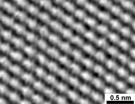
graphite as seen by an STM

Big benefit #2 of SPMs comes from the fact that you can get really creative with the probe. The image above was generated by measuring the tunneling current between an electrically conductive tip and the sample of graphite. But a different type of microscope, the atomic force microscope, generates images by measuring how much the sample deflects the probe at each point. That is, it measures the force that the atoms exert on the probe at every point in the area of interest. Other probes are designed to measure heat, capacitance, chemical nature, or a host of other properties. This makes SPMs an extremely flexible tool for doing science on a small scale.

The last major benefit is that SPMs are not limited to just looking at very small things - they can make very small things too. To see how that can be, imagine the probe as the cutter on a CNC mill. By allowing the tip to interact with what is under it the SPM can be used to precisely modify nanostructures. For example, IBM famously used one to write their name in xenon atoms on nickel in 1990:
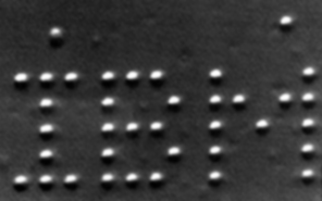
IBM in xenon

Why?

A great deal of cutting edge research nowadays in many fields, like microelectronics, biology, and material science to name a few, are only possible thanks to scanning probe microscopes. They, along with a handful of other instruments, are the Swiss Army knives of nanotechnology. I believe that a great number of our achievements as a species this century will trace back in part to the fantastical ability of SPMs to precisely measure and manipulate matter on the atomic scale. As a result, I believe that their commoditization would accomplish two great aims: 1) Lower the barrier of entry for development of nanotechnologies. 2) Speed our progress towards further technological revolutions.

How?

Scanning probe microscopes are generally extremely expensive instruments found at universities, only operated by crufty ex-industry engineers or twitchy, sleep-deprived PhD candidates. Making them cheap enough to show up on the desks of hackers and makers seems infeasible. But there are good reasons to think it can be done:

  1. It has been done before, multiple times and by different people. But not yet in a robust, reproducible way that would have direct impact in science and engineering.
  2. Lasers, optics, microprocessors, sensors, and analysis tools are all free or cheap these days. The design of Automatic Jack leans heavily on the great resources that have been brought to bear in mass-manufacturing of high technology goods.
  3. Modern computer-aided rapid manufacturing makes putting the pieces together much easier and improves the reproducibility of designs.

Challenges

  1. Touching individual atoms takes structures on the order of individual atoms. Whether they are physical probes or light waves, they need to be infinitesimal.
  2. To get atomic-scale data from probes takes mechanisms and electronics of great finesse. Atomic force is measured in probe deflections of tens of angstroms and tunneling current is in the range of pico or nano amps.
  3. A probe interacting with a single atom returning clear data above the noise is an exciting achievement, but to do useful work - imaging or manipulation -...
Read more »

automatic-jack-papers.tar.gz.gpg

gpg - 40.40 MB - 11/04/2017 at 20:47

Download

  • Voice Coil Motor Driver Built

    Owen Trueblood07/22/2015 at 18:36 0 comments

    The design for the coarse positioning stage for Jack uses two voice coil motors and a quadrature signal from two Michelson interferometers to get the fine positioning stage (piezoelectric scanner) within about 100 nm of a region of interest. By having two positioning stages using different mechanisms for their motion I’m hoping to obtain a much larger scanning area than other DIY scanning probe microscopes have achieved in the past. Instead of about 10 square micrometers for a microscope with only piezoelectric positioning, Jack should be able to cover about 1 square centimeter. Whether it’s possible to use both stages at the same time to get atomic resolution over the full square centimeter is something I want to find out.

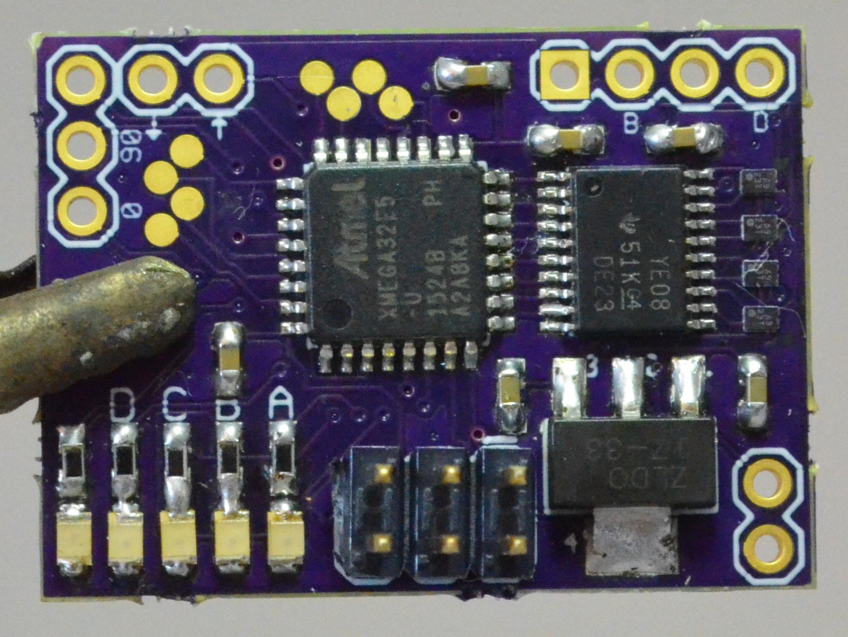
    To drive the voice coil stage I’ve designed this small circuit board. It has at ATxmega32E5 as its brains. I chose an xmega because: 1) At 32 MHz it's plenty fast for this job. 2) It has a built-in quadrature decoder. 3) I’m a big fan of the AVR family but have never tried the xmegas.

    The xmega talks to four LV8498CT voice coil motor driver chips. These are really neat ICs. They are designed for driving focus coils in cameras or phones with cameras. You give them 5 volts and instructions over I2C and they give your coils a precise amount of current up to 150 mA. I figure that they will be able to scan at rates up to a couple of kilohertz, which is good for experimentation but I’ll probably need to design my own coil driver so I can go faster in the final microscope and not have to wait a quarter of an hour per scan.

    Assembling the board was a joy, but there was some fear before I started. If you look at the right side of the picture of the assembled board above you’ll see the four coil drivers. You might be confused and think, “how is that a whole driver IC? Those parts are smaller than the 0603 resistors and caps on the rest of the board!” The reason the drivers are so small is that they are in wafer-level packages. This means they are actually tiny slivers of silicon without the usual epoxy packaging (the picture doesn’t show it, but they sparkle beautifully in the right light). There are 6 miniscule solder balls on the bottom of each for the connections. I was not sure if OSH Park could even meet the specs for the package, let alone if I could solder them. But as it turns out you can just lay down some flux, forget the solder paste, position ICs with a needle, and go at them with a hot air gun. The little guys align themselves thanks to surface tension. Since the pads are accessible from the edges the tiny errors in the board fab don’t matter.

    Next update will come when I write the first version of the firmware for this board and have some coils moving. I’ll be at Artisan’s Asylum tomorrow night if you’re going to the HaD Boston meetup and want to ask me about this project!

View project log

Enjoy this project?

Share

Discussions

Mohammed wrote 12/13/2018 at 16:27 point

Very nice project, how did it advance?. I am planning to build a xy nano-precision stage and trying to get ideas. I was also trying to download the project file, but it needs a password, may I have it?

  Are you sure? yes | no

Dan Berard wrote 07/25/2015 at 15:52 point

Very cool project. I like the dual-stage scanner idea, although it might be difficult to get the rigidity and stability required for atomic resolution. Good luck, looking forward to seeing how this turns out!

  Are you sure? yes | no

Owen Trueblood wrote 07/25/2015 at 16:16 point

Thanks! I agree that rigidity and stability are going to be difficult properties to achieve. My strategy for rigidity is to add mass and use flexures cut out of metal or thick plastic to hide material imperfections. I'm also looking into active stabilization, because although it is complicated to design if it works it will make the project much more reproducible (shifting complexity from tricky-to-machine parts into copy-able software & circuitry). For stability I'm going to implement a temperature control system (closed-loop acting on water). And passive vibration cancelling will come from mass & spring (mass from the water used to temp control and spring in the form of an inner tube that the whole system rests on).

edit: I didn't recognize your name and then I looked at your project page. Your scanning tunneling microscope blew my mind when I first saw it and directly inspired my project. Thanks so much for putting your work online!

  Are you sure? yes | no

Dan Berard wrote 07/25/2015 at 21:36 point

Sounds good, although the water is probably unnecessary. A closed box with some heaters should do the trick. I bet temperature control will help a lot with stability. Once you get it up and running, maybe you can replace the water with liquid nitrogen :)

  Are you sure? yes | no

Similar Projects

Does this project spark your interest?

Become a member to follow this project and never miss any updates