ben biles
-
weird DAC output fixed
11/30/2023 at 10:00 • 0 commentsI must have blown the DAC by inserting a car incorrectly at some point.
changed the DAC IC and its sounding GREAT!!
I have the balanced outputs going into a Tascam LA40 mk2 so I can listen to the outputs on monitors and I'm using an old Behringer 4 channel Ultra Pro DI rack for testing mixing lots of channels at the same time.
The idea is I actually use this box for PC TV Alexa and whatever rubbish I use at home to test long term stability. does it crash , over heat and all that ! so far so good.
I've set the main faders to mix from -inf dB to +16dB and the main output faders from -inf dB to +18dB
-
Line Driver buffer clipping
11/27/2023 at 00:27 • 0 commentsI have only just found time to check the differential line drivers cards. They are way off !!
I have clipping on one side.
I have measured after the DC blocking caps between the biased buffer op amp and the line driver IC ( That 1606 )
I think I need to check what's happening before the blocking caps now and try and figure out why the output of the buffer opamp is 1.25V peek on one rail and clipping at 1V on the other !
-
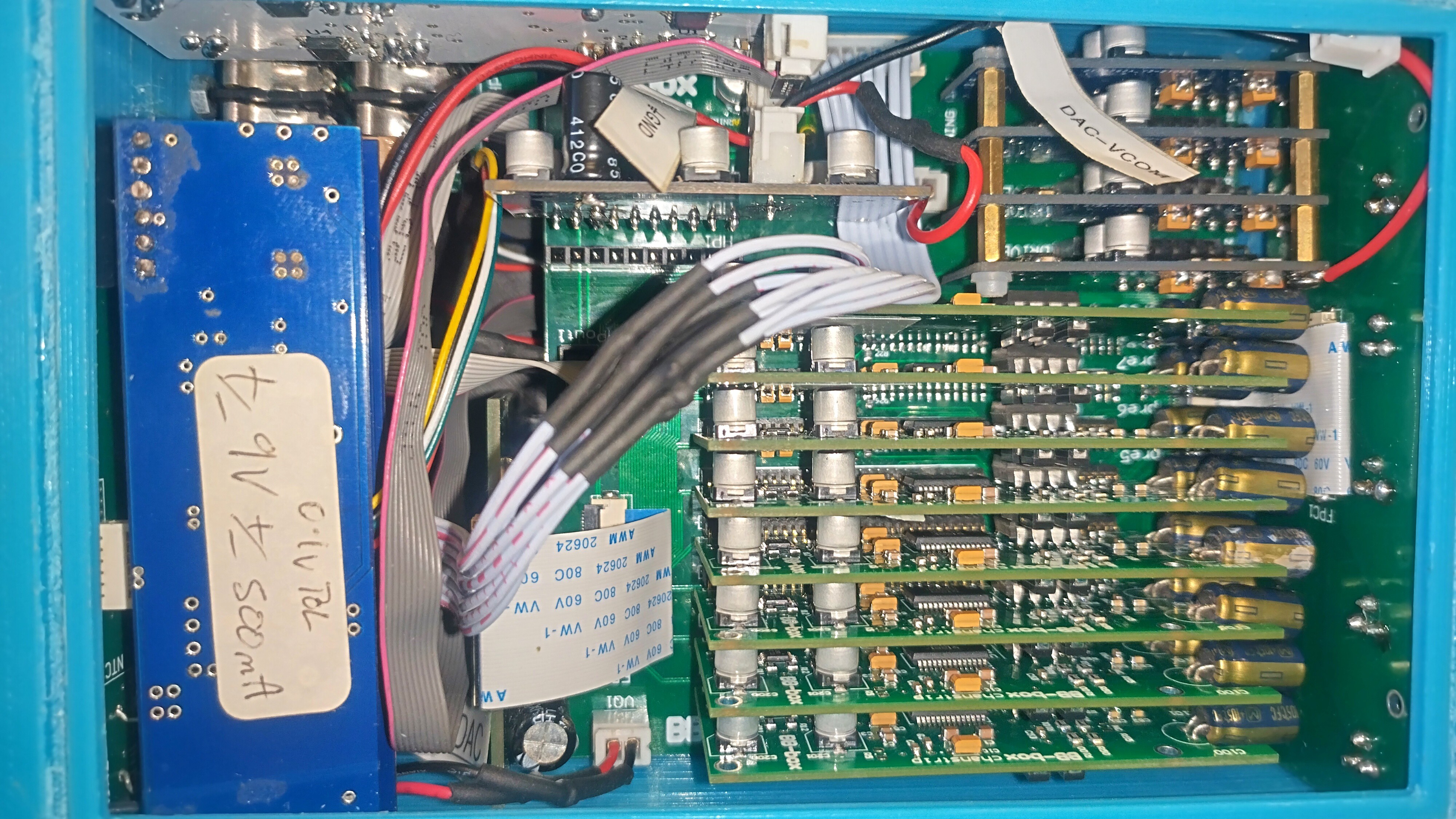
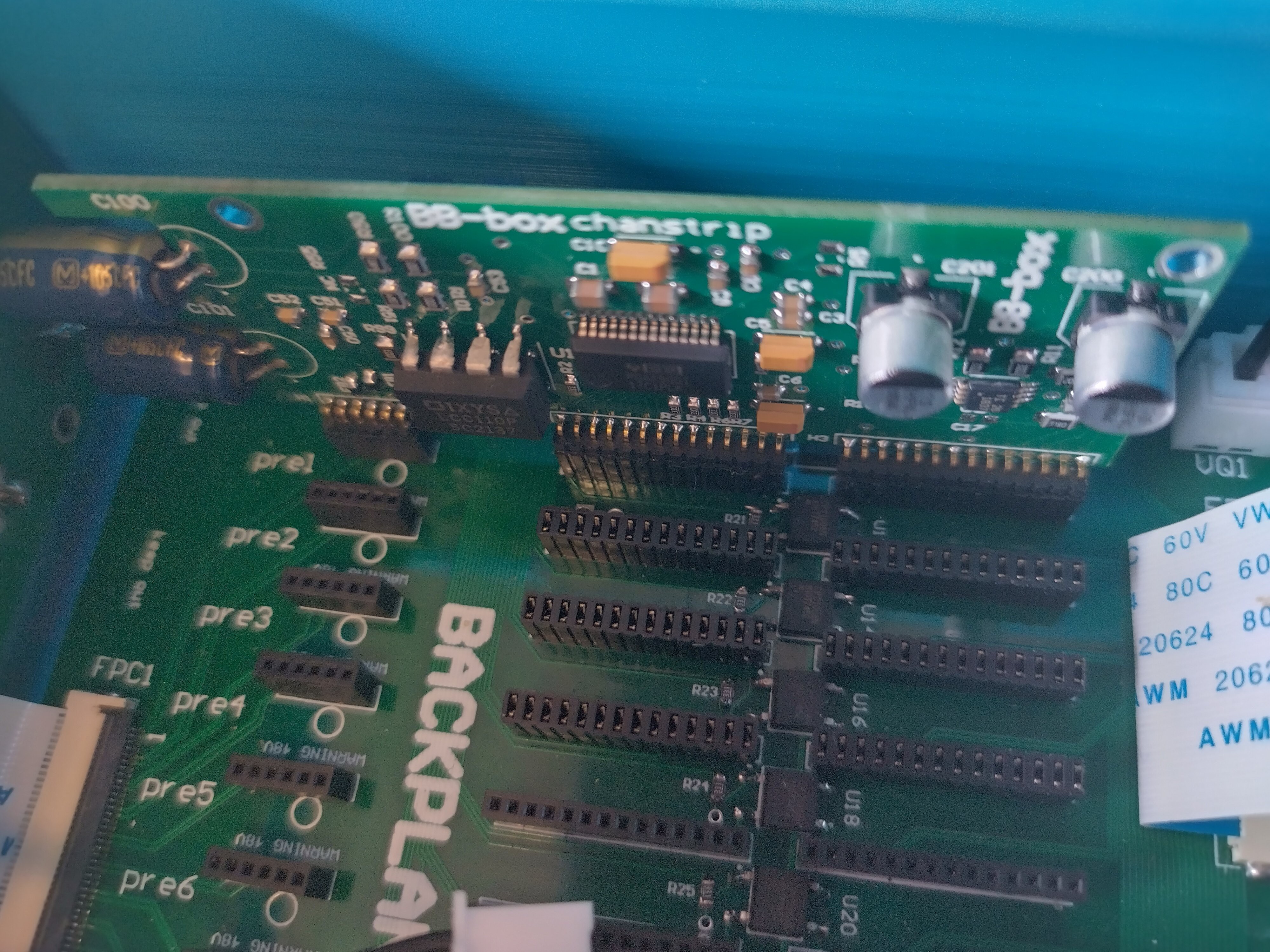
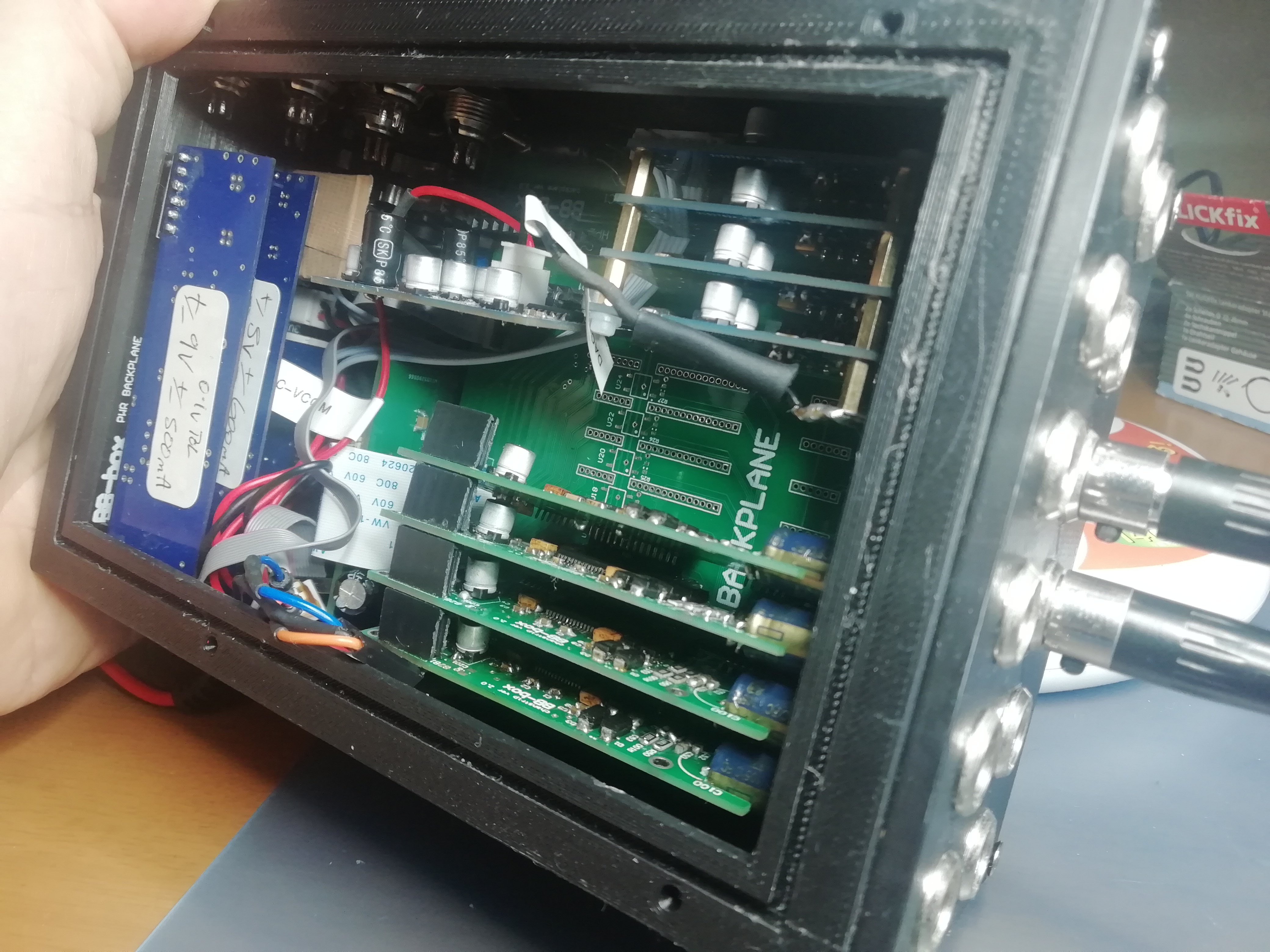
8 pre amp cards loaded !
03/19/2023 at 18:18 • 0 commentsHere's a pic of all 8 preamp cards with 4 balanced line driver card loaded.
The headphone card gets warm , so I'm only running 1.
The protection diodes on the rear of the preamp cards are in the way of the SMD electrolytic caps ( they moving over about 10mm )
They were added to protect the PG2500's against voltage rail error !
The next job is to code the +-5v rail monitoring on the MC and have all the channels immediately shut down if there is a
voltage rail deviation > 0.1V
The would have preferred there protection diodes to be on there too ! next revision I'll move them over 10mn so they are well
clear.
This is all part of learning how to build multi board designs !
The gap between the balanced line drivers and preamps is tight but ok.
you can see the analogue IO panel FPC connector just fits.
I'm thinking of stripping a lot of the 3d printed box away so it's just a frame and then
using aluminium panels to make up the sides and connector panels of the box.
![]()
-
my 1st manufactured PCB cards !
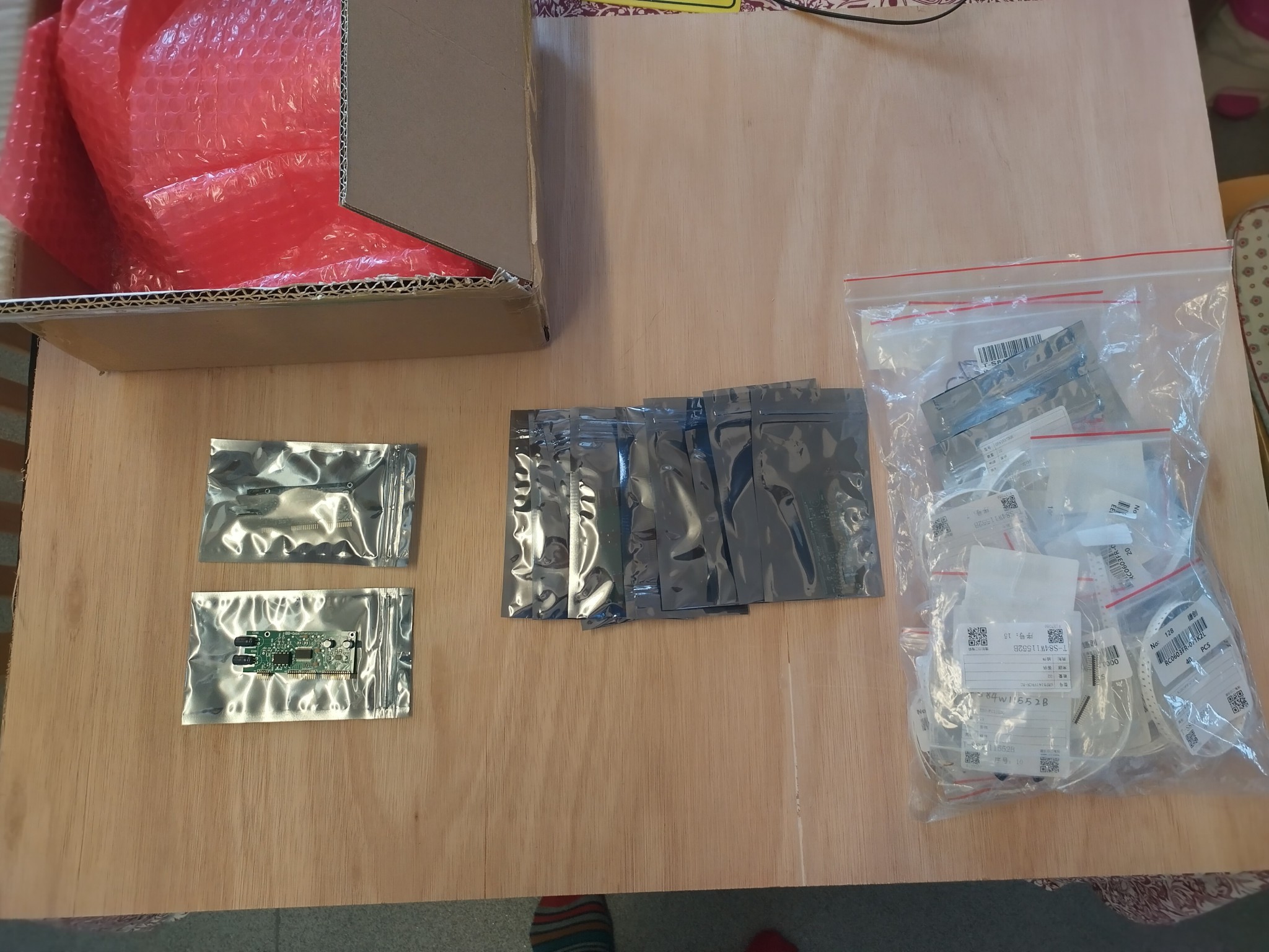
01/08/2023 at 15:54 • 0 commentsExciting times :) !! I have ordered my 1st run of cards at PCBway pick and place !
![]()
Here are my 1st ever professionally manufactured boards :)
There are only 10 cards , but the parts are not cheap !
https://www.pcbway.com/assembly-process.html did an amazing job here guiding me through the world of having a correct BOM ( bill of materials ) and checking everything from part orientation to proper part / footprint matching !
They part sponsored the project by reducing the pick n place / manufacture cost by 50% which was really helpful. This is not why I am writing a positive review about them though. I am free to write what I want here !
They really did have a ton of patience with me and my stupid mistakes on this. I can't recommend you use this service enough if you have never had a board professionally manufactured. You can send your own parts or have them source the parts locally. some parts I had to send them as they are difficult to source in China due to the current situation. but its easy to send parts directly to them.
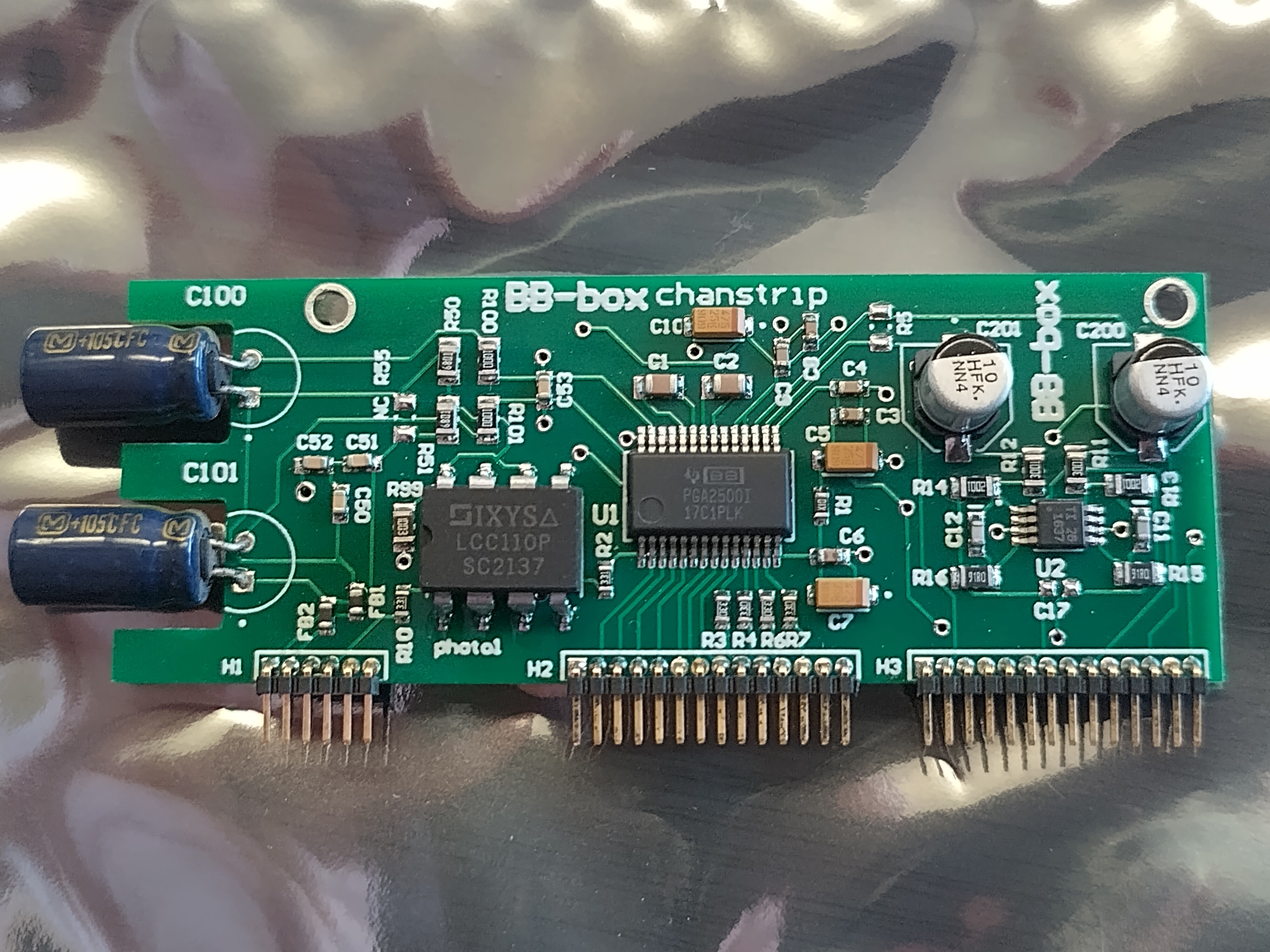
On this version of the preamp I have VCOM from ADC coming in through the connectors.
I also reduced the size of the phantom blocking caps as it was taking to long to drain them and causing problems with the PGA2500. The lower value 22uF blocking caps should slightly increase bass filtering slightly but so far I can't tell the difference from using these or the 47uF blocking caps. apart from the faster drain time when phantom power is switched off. When phantom power is switched off or on the DSP mutes the inputs for 1 second in case of large banging noise etc. this time was reduced using the smaller blocking caps.
I need to glue the caps onto the PCB myself but I opted to do this myself to save time.
As you can see the solder reflow is really nice !!! especially on the PGA2500 and OPA1637
![]()
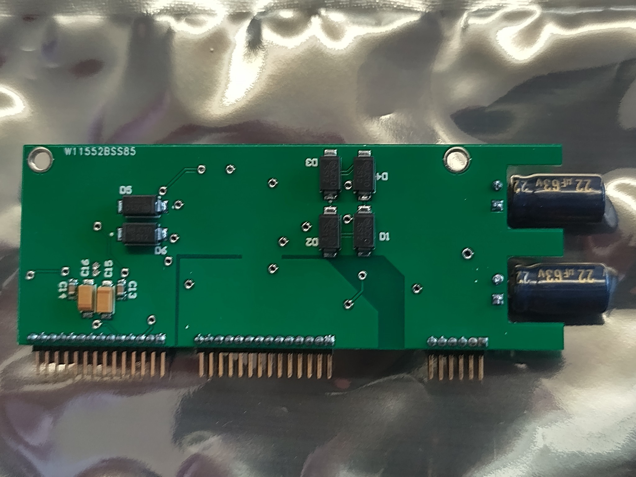
diode protection on rear for power protection and phantom power short protection
![]()
One thing I can say , using KiCad you often just choose a generic symbol / footprint for resistor or capacitor etc and have in the back of your mind what actual part you will use. this is really bad practice since when you output your BOM there are to many empty holes as far as manufacturing are concerned. it might be just a 10k 0603 resistor to you , but they need to know exactly what part to order for you !!!!! its so easy to overlook when outputting a BOM ! worse still a really bad habit of mine is to just use say a resistor footprint for say a capacitor or ferrite bead !! don't do it !! you will forget and the factory could easily choose the wrong component.
Anyway , thanks to PCBway they fixed my stupid mistakes and got me some really nice working preamps for the BBBOX mixer recorder.
here's a few pics of a card inserted !
note , FPC cables to ADC/DAC card and ext connectors to :)
![]()
![]()
-
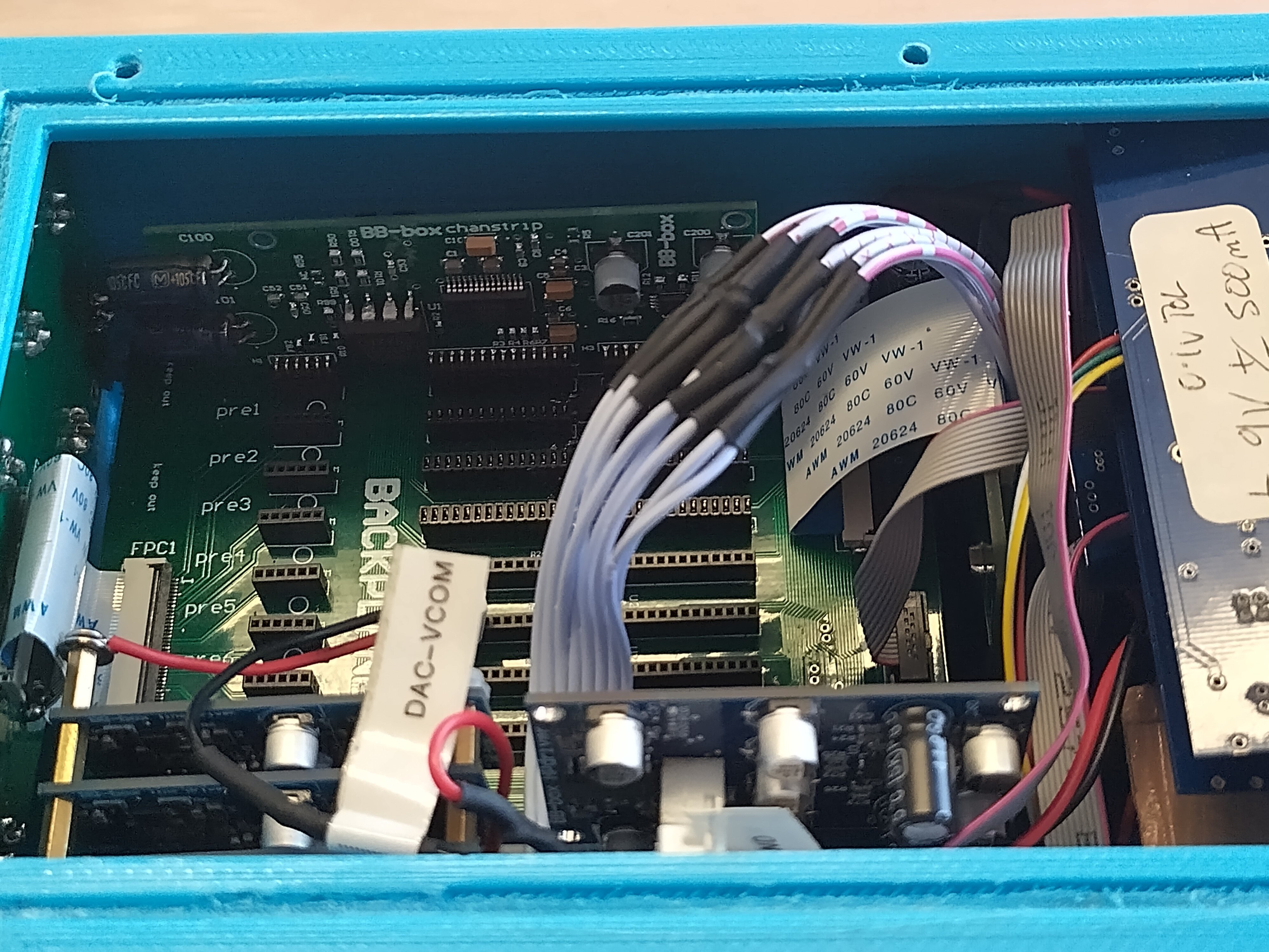
switching battery / ACDC adapter testing
12/01/2022 at 10:40 • 0 commentsSEE PREVIOUS LOG FOR DESIGN NOTES
Its working but next revision I think I will change the priority to the mains ACDC power input if both battery and wall adapter are plugged in! basically swap the 2 power input wires around :)
-
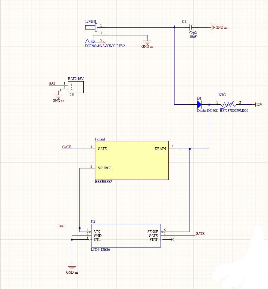
battery to dc wall adapter switch !!
10/17/2022 at 04:13 • 0 commentsit never ends !! :)
now I need a battery / acdc wall adapter power switch. I'm not charging the V-lock battery's on board as people generally use there own proper chargers.
I also include NTC protection [ edit , PTC resettable fuse , not NTC ! ) ] in case there is ever a short somewhere !!
I'm going to try using the LTC4412 to switch a BSS308 ( P channel mosfet )
more cost and more complexity !
![]()
does anyone know of a cheaper simpler way that takes up little pcb space ?
I could just switch the mosfet with the mechanical DC barrel jack switch but seams a bit risky ?
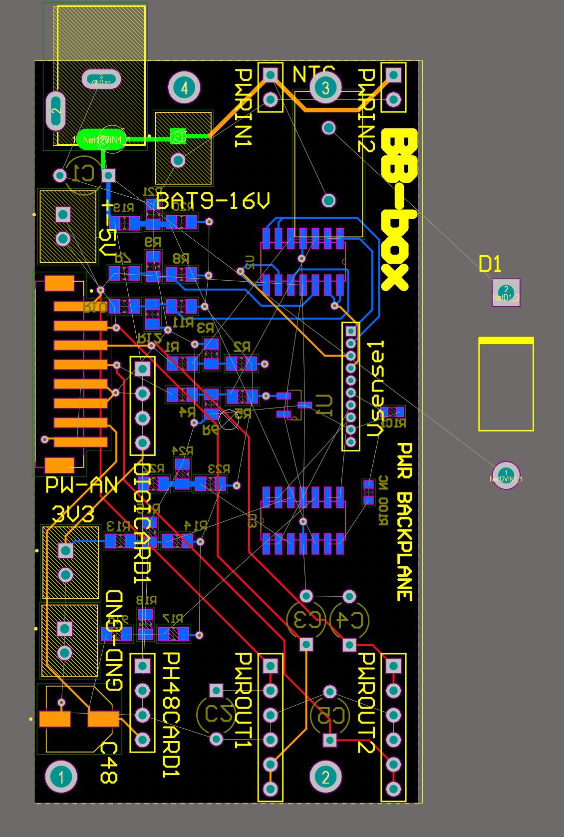
My backplane is already pretty loaded with voltage level monitoring / ADC buffering so I'm making it 4 layer this time and with components will be on both sides. the vsense1 socket will send the buffered 0 - 3.3v voltages to the MC. the digi main board only has 6 ADC channels hooked up at the moment but eventually that will be upgraded to 8 , that way I can monitor battery Vin ( DC vin ) +-15 +-5 48v 3.3v and more
![]()
the diode in this example obviously doesn't fit this design !! I'm sure I will find a decent heavy duty
SMD version.
ahhhh , I'll make it all fit , there is always a way !
-
BB-Box gets a V-Lock pro battery 99 W/h , plane safe !
03/14/2022 at 07:48 • 0 commentsBB-Box gets a V-Lock pro battery 99 W/h , plane safe !
-
preamp / line driver and HP cards in with +/-9v opa1637 buffers biased from VQ on ADC and DAC
10/06/2021 at 13:38 • 0 comments4 preamp cards and 4 balanced line drivers using OPA1637.
The Vcom and higher +/-9v rails for OPA1637 buffer are supplied through the stackable headers on the preamp cards. They are 1mm to long so not sure I will be able to squeeze all 8 preamps in there using those.
The 6mm brass standoffs worked fine for the line drivers and I send the VQ down one line of brass standoffs and it works.
![]()
-
more work on the chassis / box
09/26/2021 at 12:18 • 0 commentsI've started work on the case again and will print another in CF and will glue on some thin aluminium panels in recesses in the CF.
I am making plates for connectors that bolt to the chassis. so far only 2 plates , 1 for the mini XLR inputs / outputs and 1 panel for the AES IO mini XLR and 1/4" headphone sockets.
I made some slots in the digital and analogue main board mounts so I can slide in some EMI shielding between the 2 boards.
this is a very rough 3d thing of the assembly. you can click to make a cutaway.
-
more work on the chassis / box
09/26/2021 at 12:18 • 0 commentsI've started work on the case again and will print another in CF and add some aluminium panels.
I am making plates for connectors that bolt to the chassis. so far only 2 plates , 1 for the mini XLR inputs / outputs and 1 panel for the AES IO mini XLR and 1/4" headphone sockets.
I have no idea if this 3d grab cad page will embed but its a rough idea!
Multichannel Audio DSP Field Mixer Recorder
bluetooth app controlled professional portable DSP mixer.balanced audio IO,phantom power,flexible routing,ISO recording. timcode. AVB audio.