 Ted Yapo
The Clock
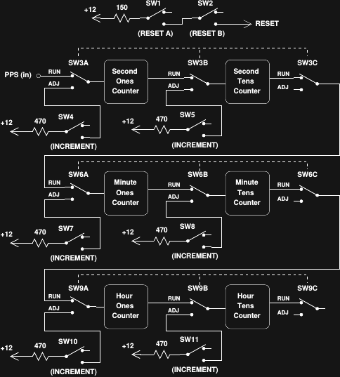
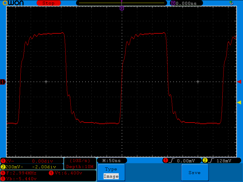
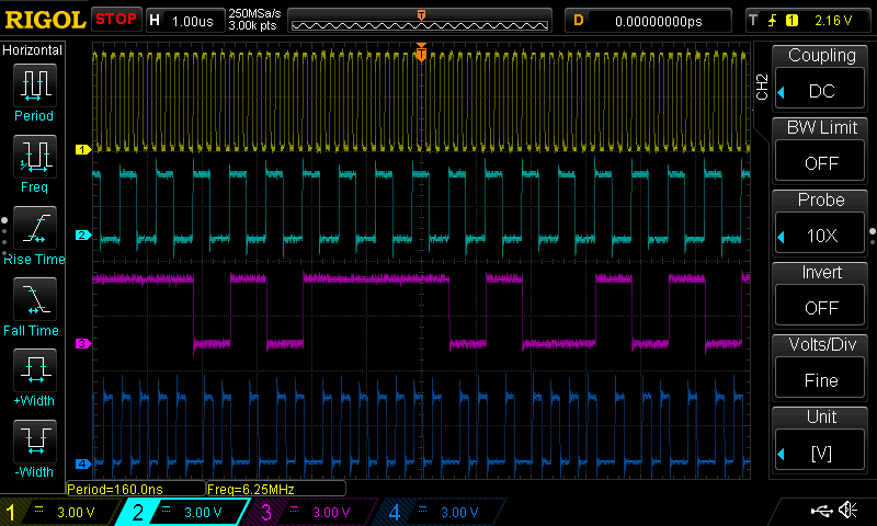
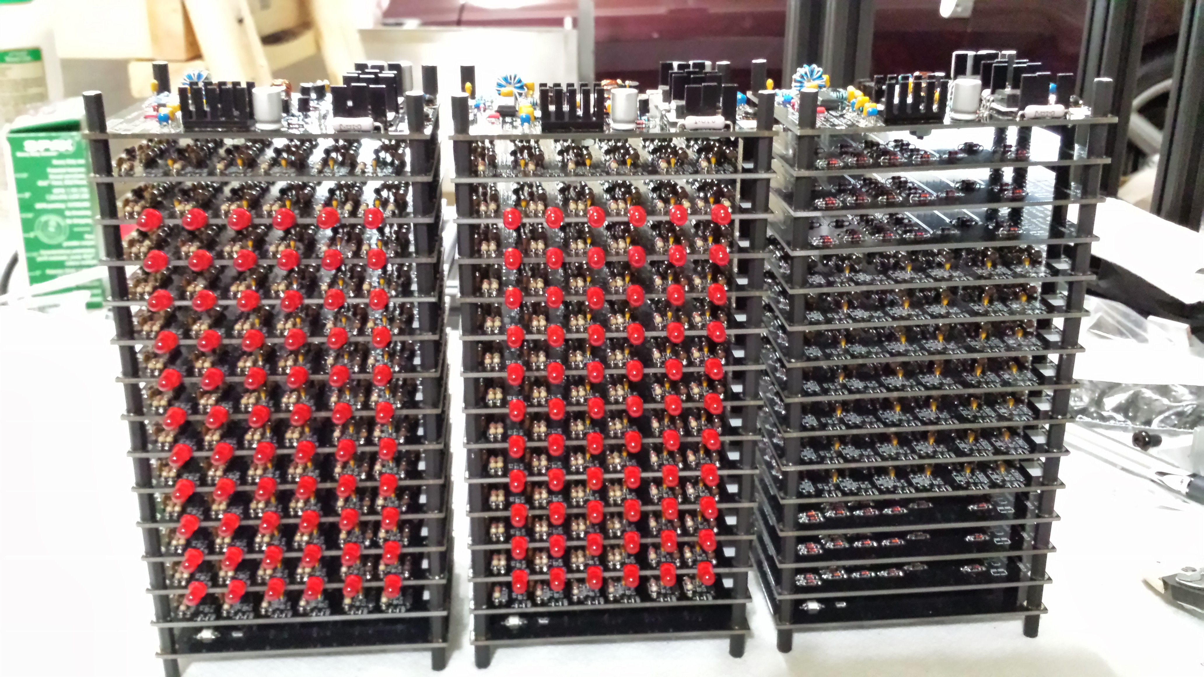
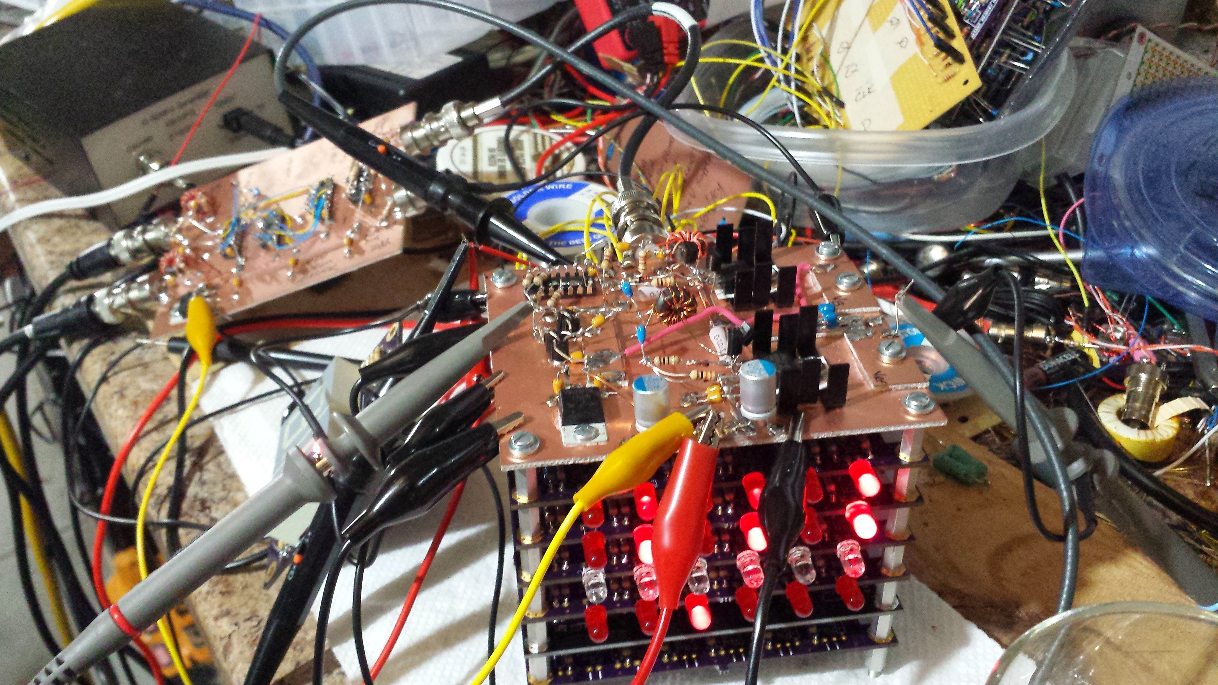
The clock is a six-digit HH:MM:SS timepiece using only DDL gates (1N4148/1N4007 diodes) for the logic and display functions (the LEDs are also diodes, of course). The power supplies and currently the crystal-oscillator timebase use more traditional circuits, including transistors and ICs. You can see the clock working in this brief video:
IMPORTANT: I've added a Builder's Notes log section for details and errata about the project for those experimenting with DDL or building their own clock. Please read before you begin.
Diode-Diode Logic (DDL)
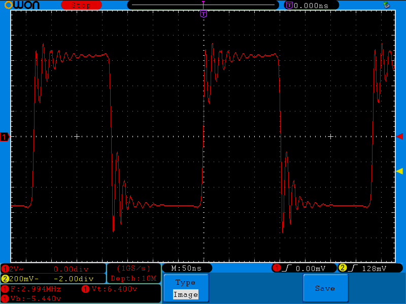
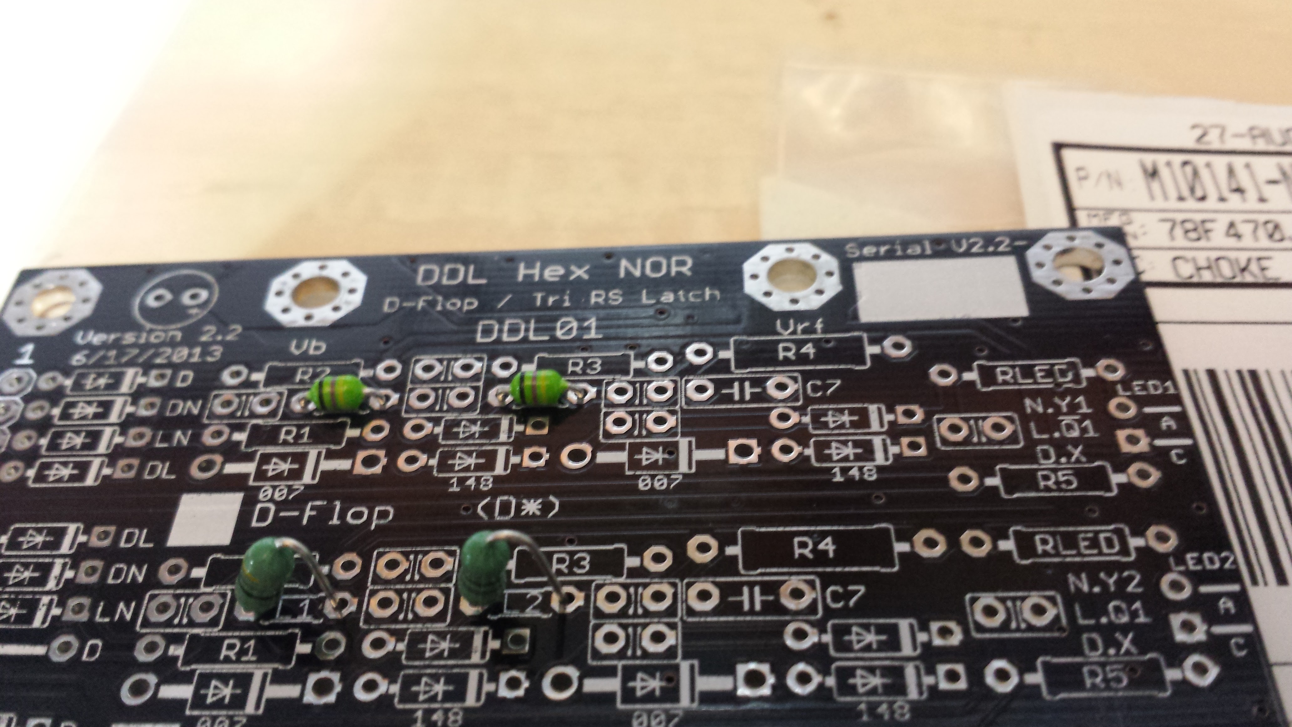
DDL is an idea for building complex logic systems, like digital clocks or computers, using only solid-state diodes as switching elements. In the current version of DDL, a 1N4007 diode forms an inverter by switching radio-frequency current based on logic-level signals. Combined with a 1N4148-based OR gate, this makes a NOR, from which any combinational or sequential logic function can be constructed. Modular circuit boards have been designed and proven, so that working with DDL can be (almost) as easy as using TTL or CMOS logic. Just grab the DDL01 datasheet and start designing!
If you want to build something now, check out the simple demo circuit. You probably have the parts sitting on your workbench.
Like building contemporary logic circuits from individual TTL gates, discrete transistors, or relays, DDL is at its heart a perverse technological pursuit: an artificial challenge in an age of effortless gadgetry. So, have fun with it...
Goals

The ultimate goal of DDL is to build a simple computer using only diodes as logic elements.
The Diode Clock project is a first large-scale test to see if the idea scales to "real" systems. It does. 276 diode NOR gates are combined to make the clock, providing reasonable proof that a simple computer could be assembled. The reality is that a clock built with DDL is more useful than a computer that could practically be built with the current iteration of the "technology."
We live in the transistor-computer age. At some point, our current computing technology will join the vacuum tube, the electro-mechanical, and the mechanical computing devices in the technological trash bin. DDL isn't the next computing technology (I can assure you of that), but it's time to start thinking about what will be.
DDL Devices
I've designed several PCBs enabling any digital logic circuit to be constructed using diode logic. These are all released under the CC-BY-SA license. After I've finished documenting it all, I'll release everything in one central GitHub repository. For now, grab files here:
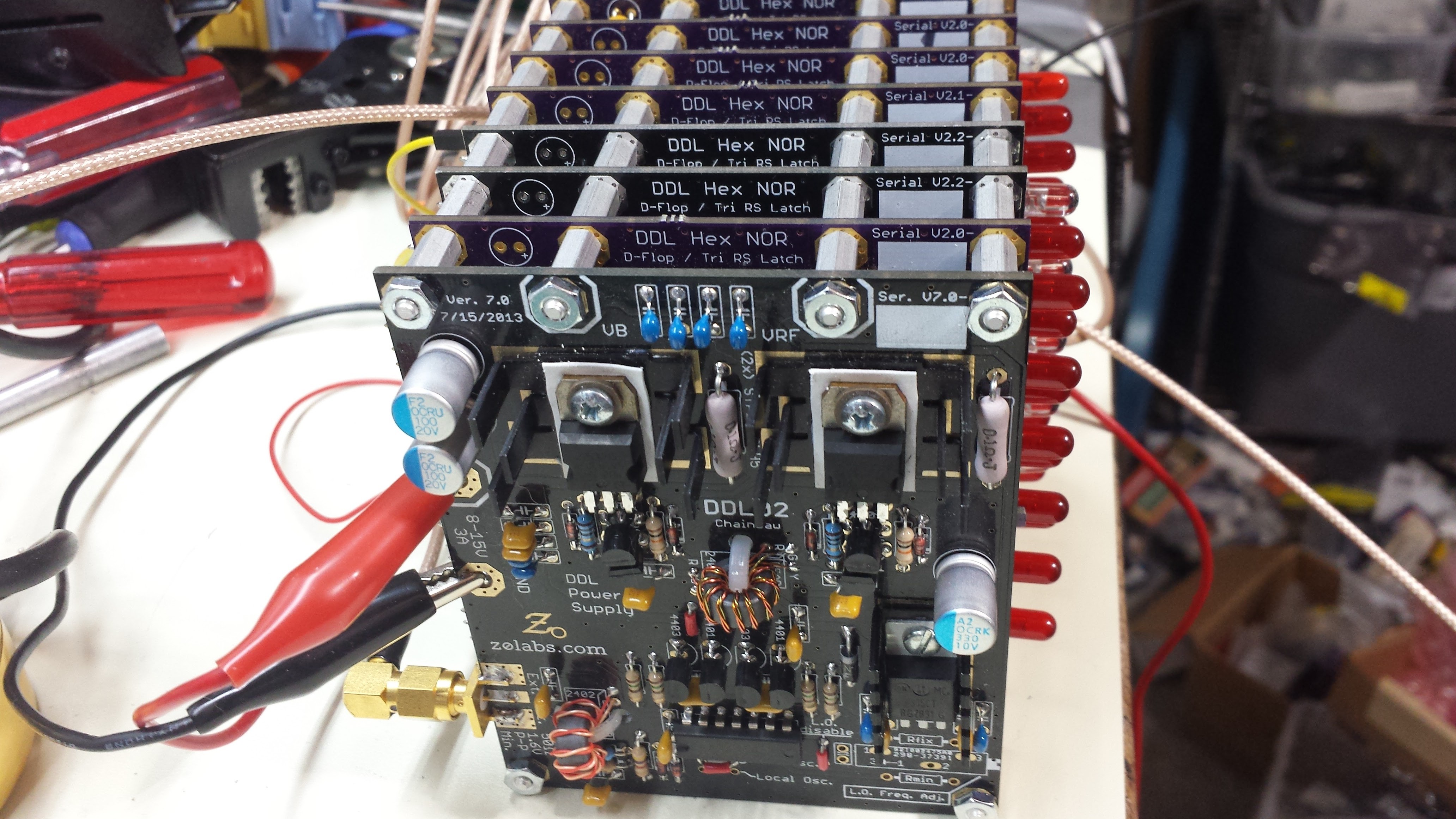
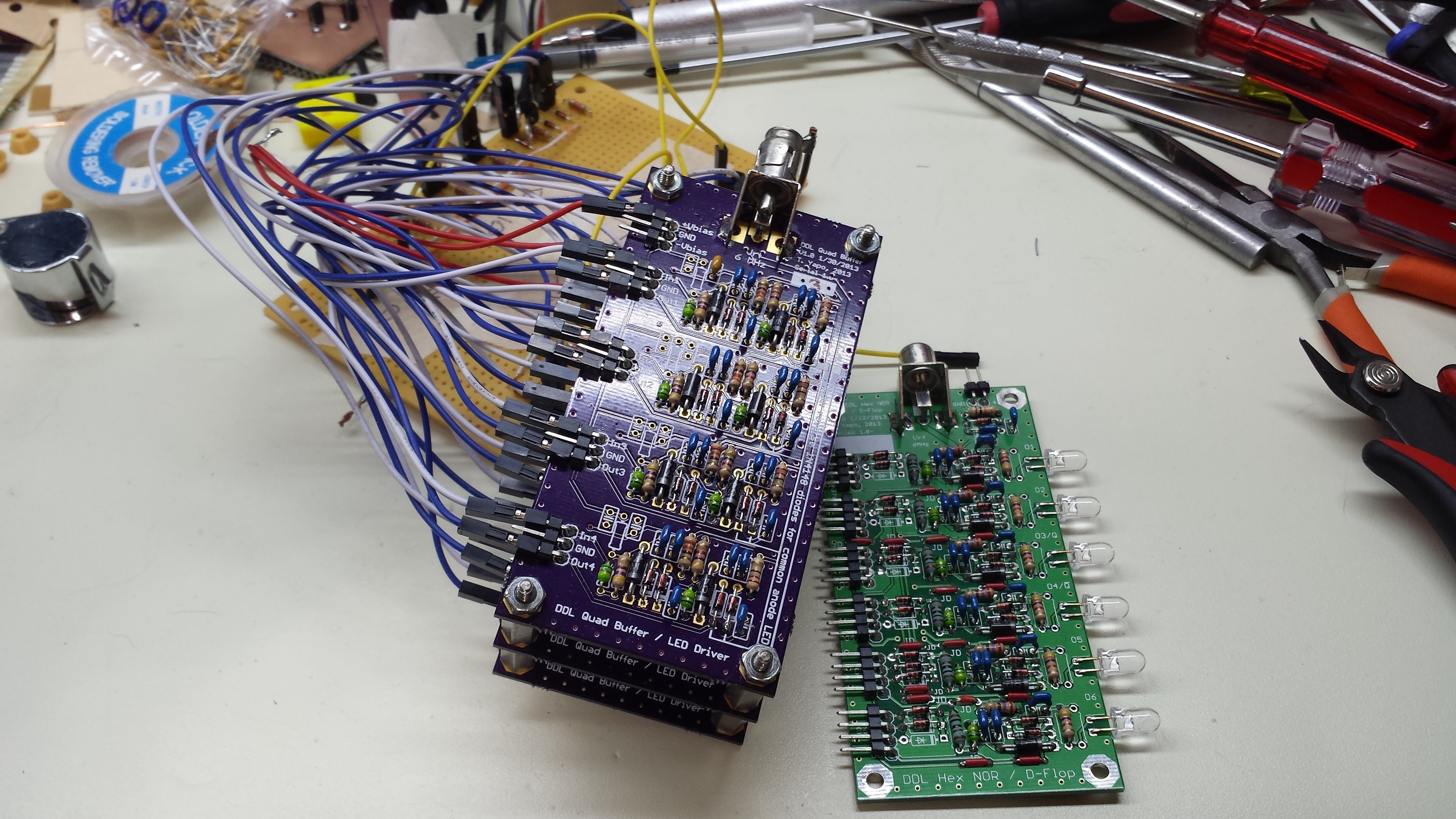
- DDL01 (datasheet, LTspice simulation, design files, project log, OSH Park): Hex NOR Gate. Basic DDL building block. Can alternatively be configured at build-time as a triple RS latch or single negative-edge-triggered D flip-flop.
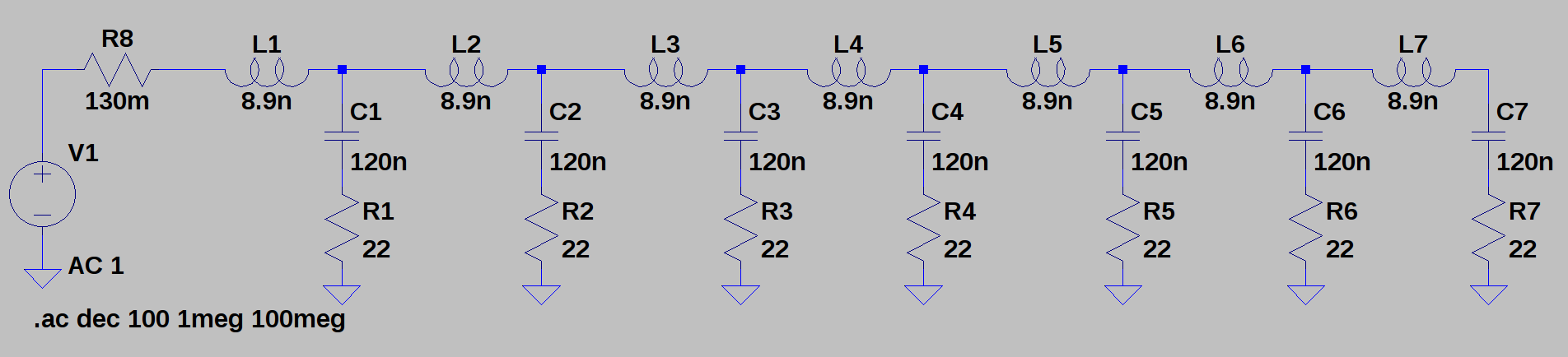
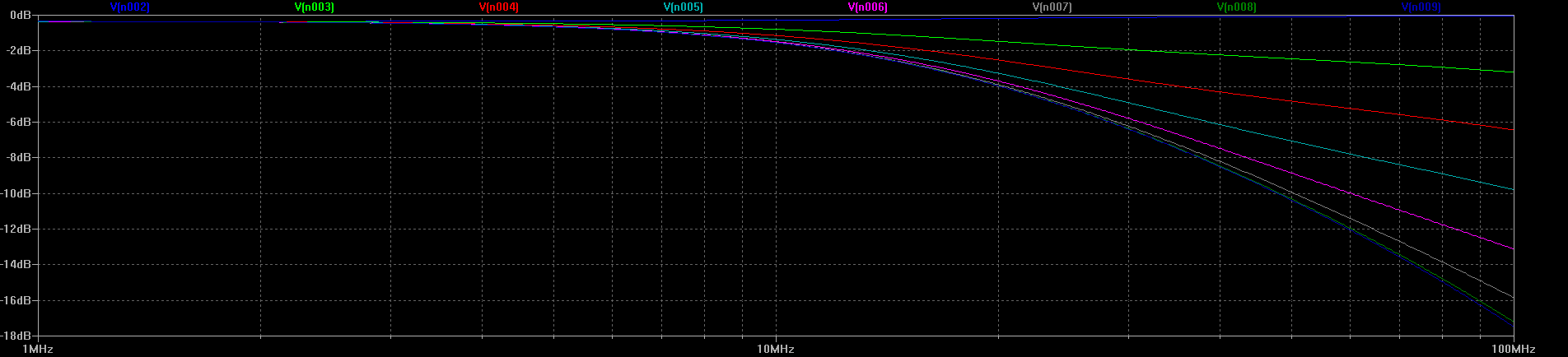
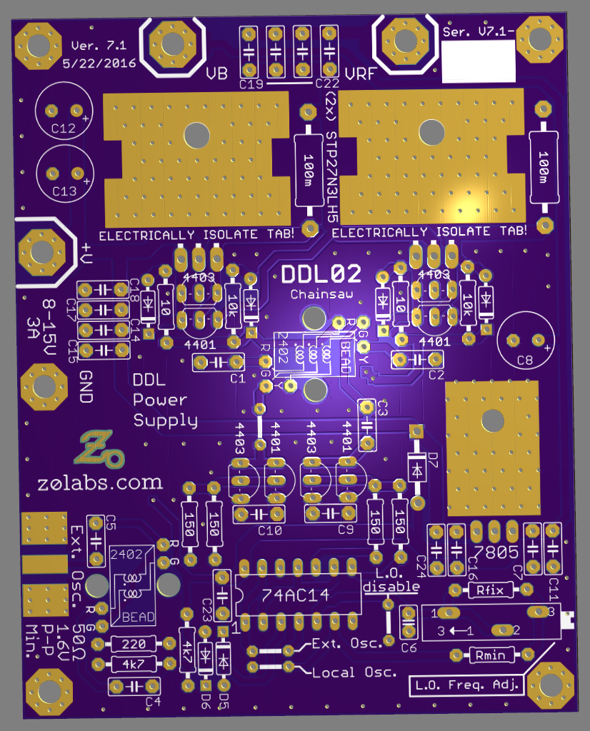
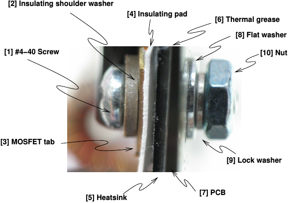
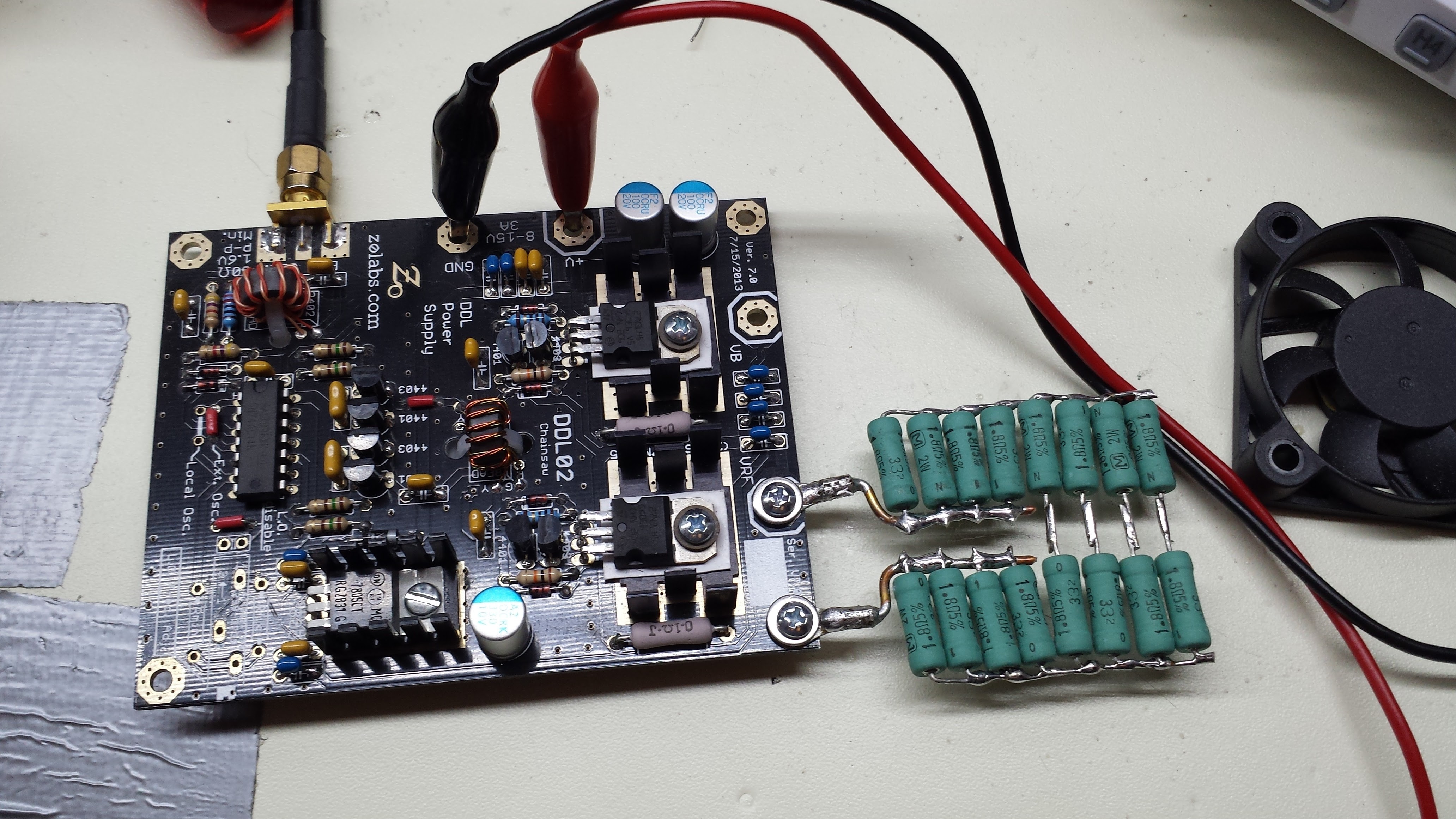
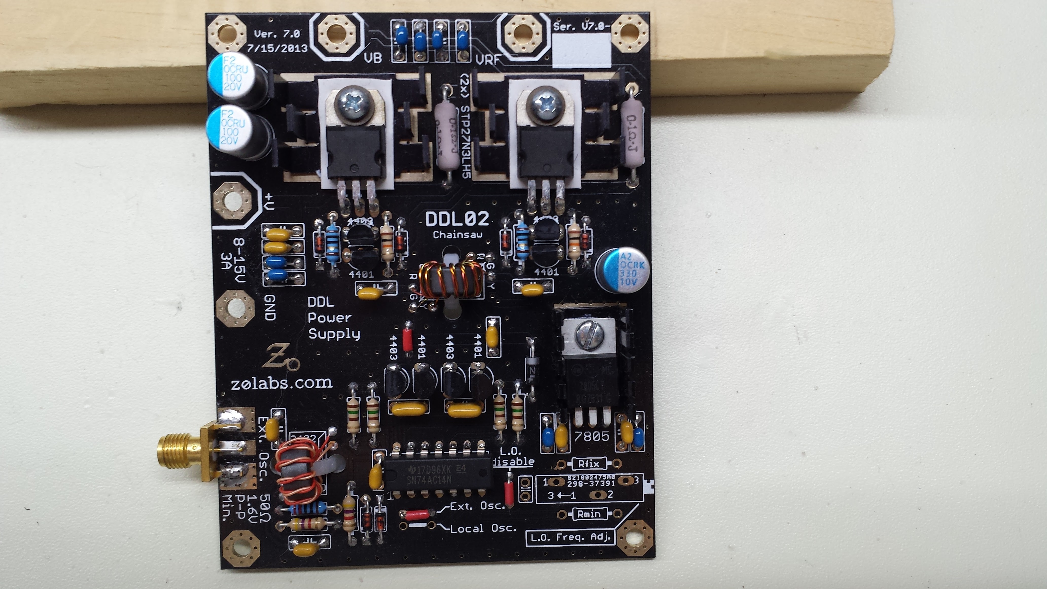
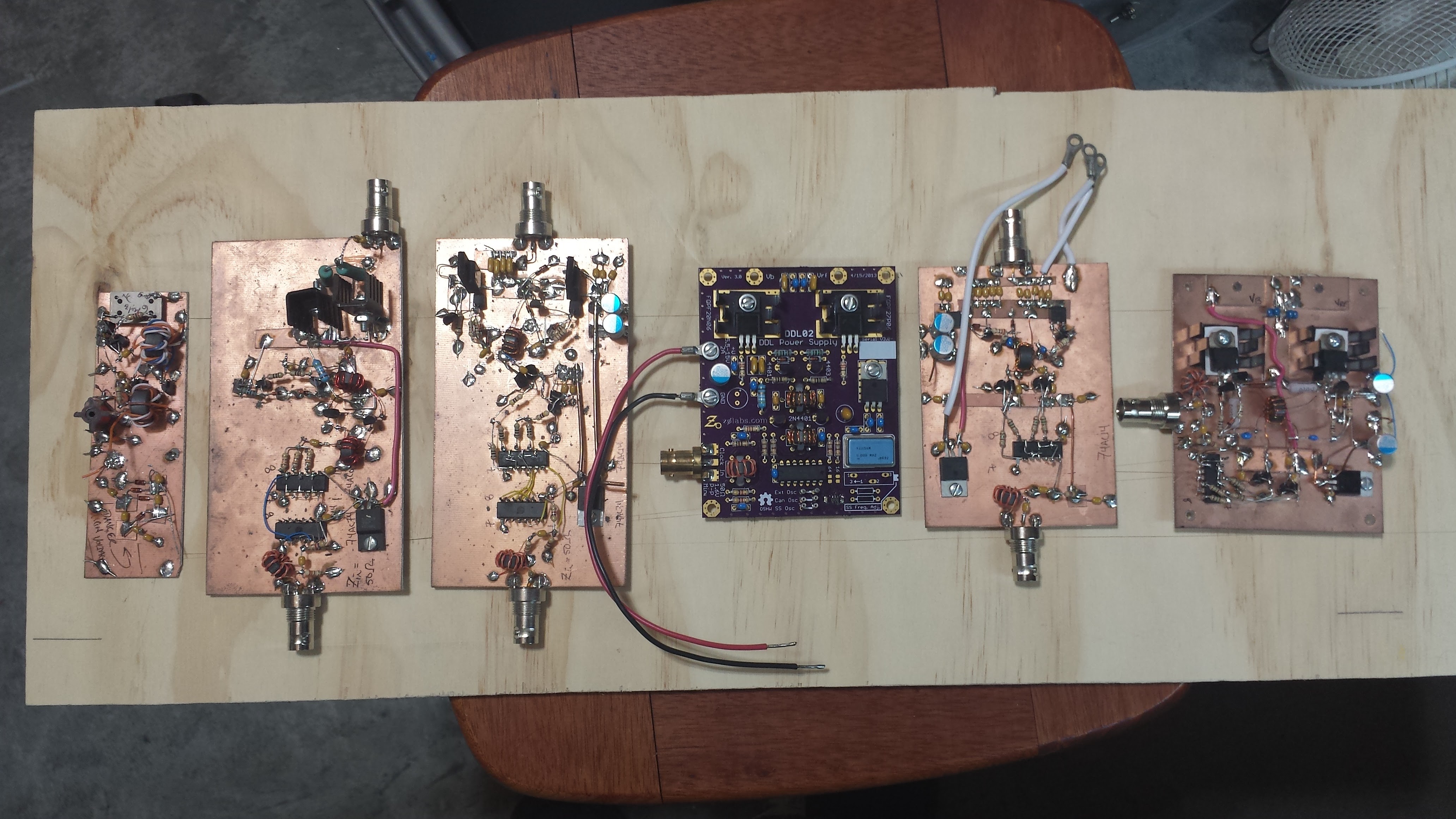
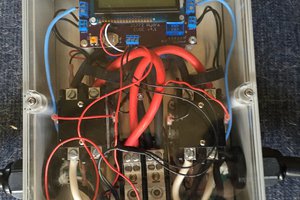
- DDL02 (schematic, LTspice simulation, project log[1], project log [2], design files, OSH Park, BOM): "Chainsaw" RF and DC bias power supply board. Runs on 12V and provides the low-impedance RF power (up to 35W) required for DDL logic. Supplies up to 20 DDL01 boards.
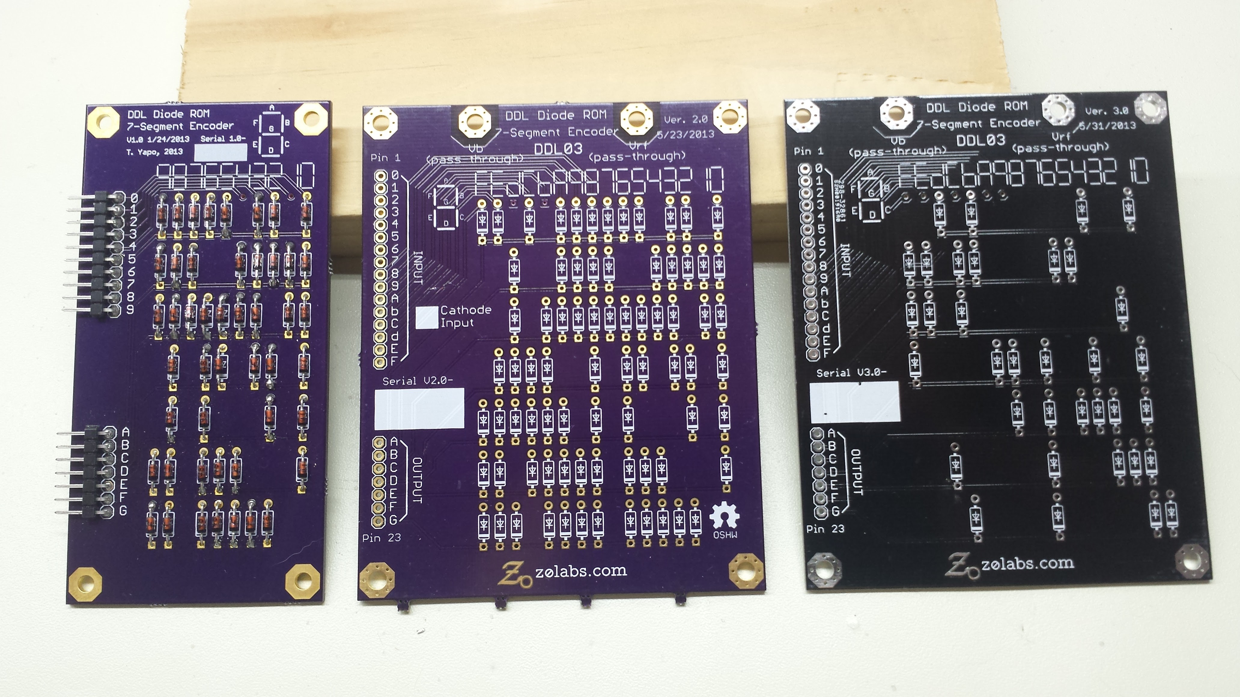
- DDL03 (design files, OSH Park): Hexadecimal-to-7-Segment Diode ROM Encoder. Encodes hexadecimal digits for display on a 7-segment LED.
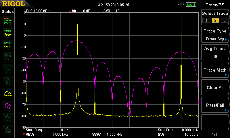
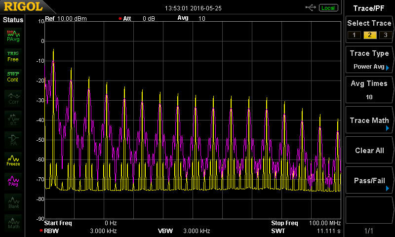
- DDL04 (design files, OSH Park): "Whisper" Spread Spectrum Exciter. Used to generate spread-spectrum RF for the power supplies to reduce RF emissions.
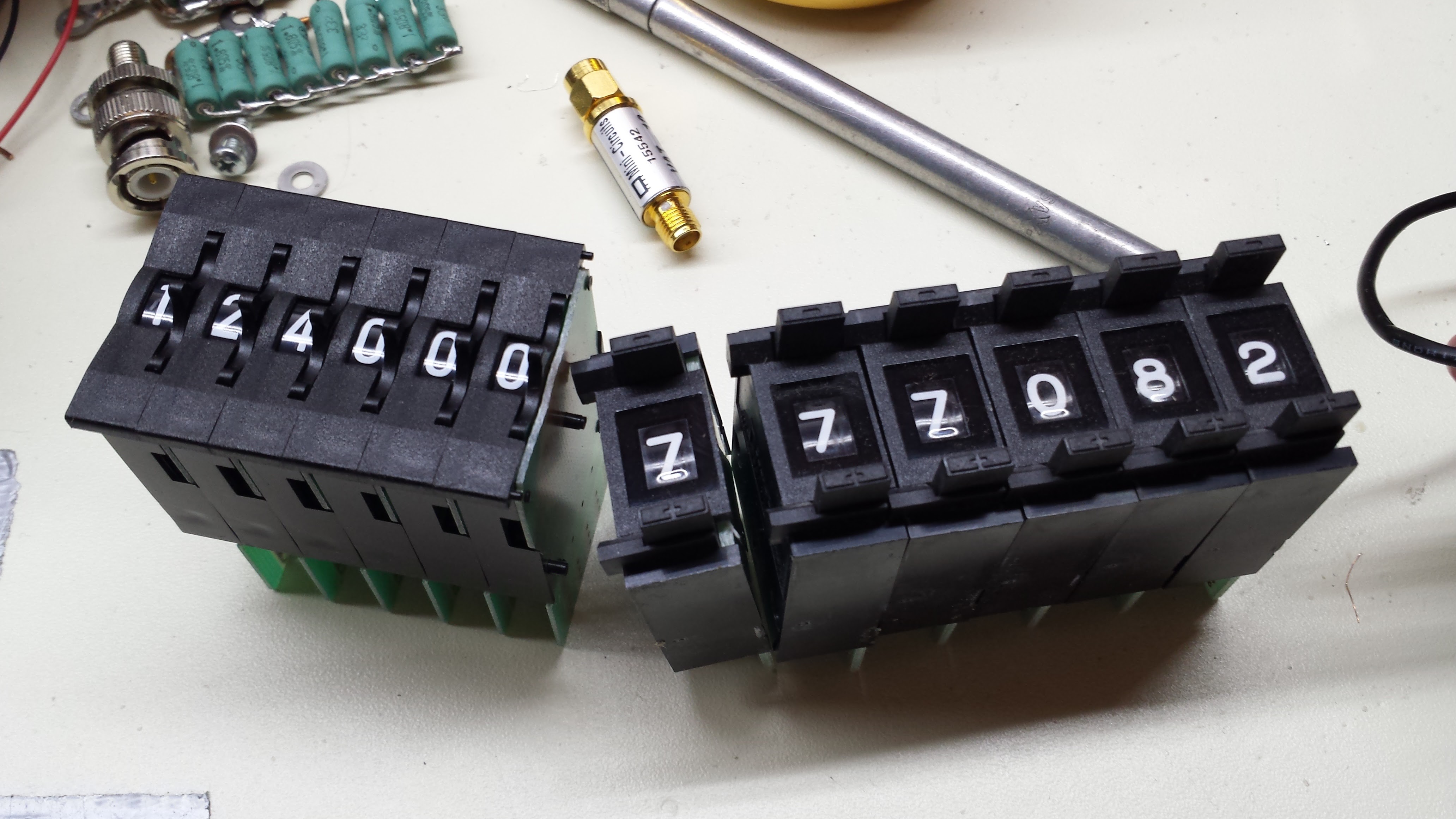
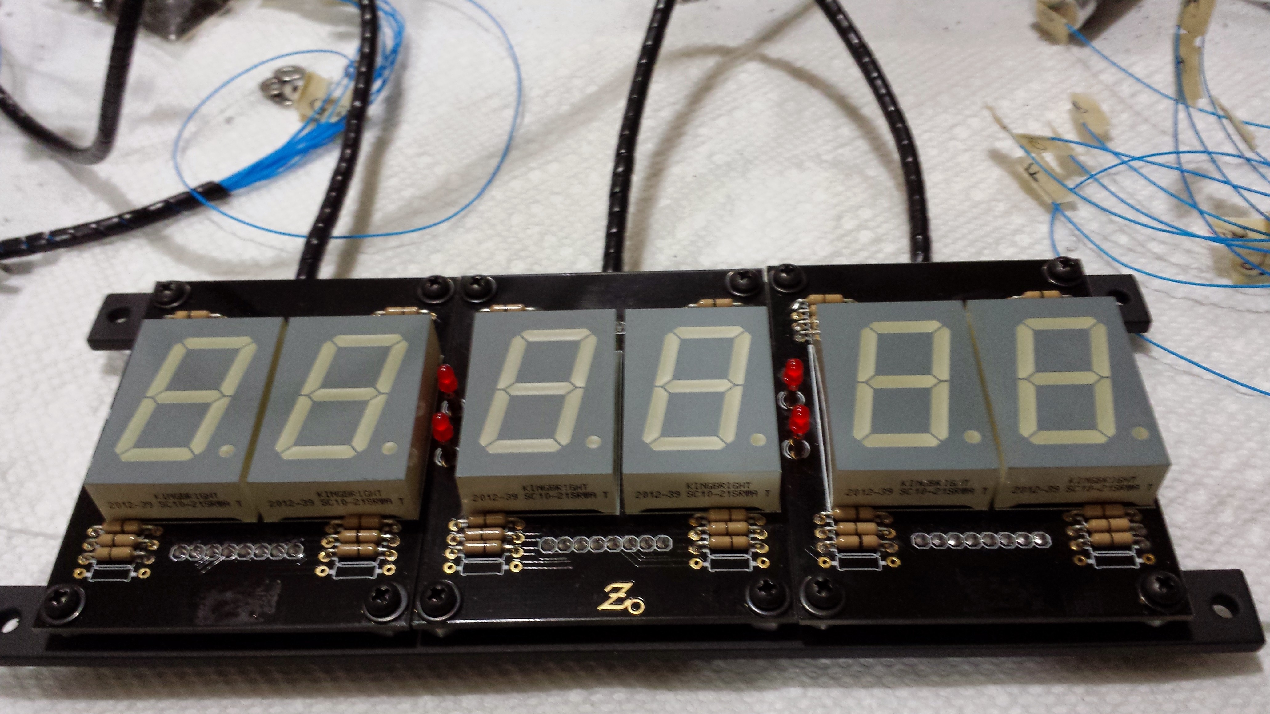
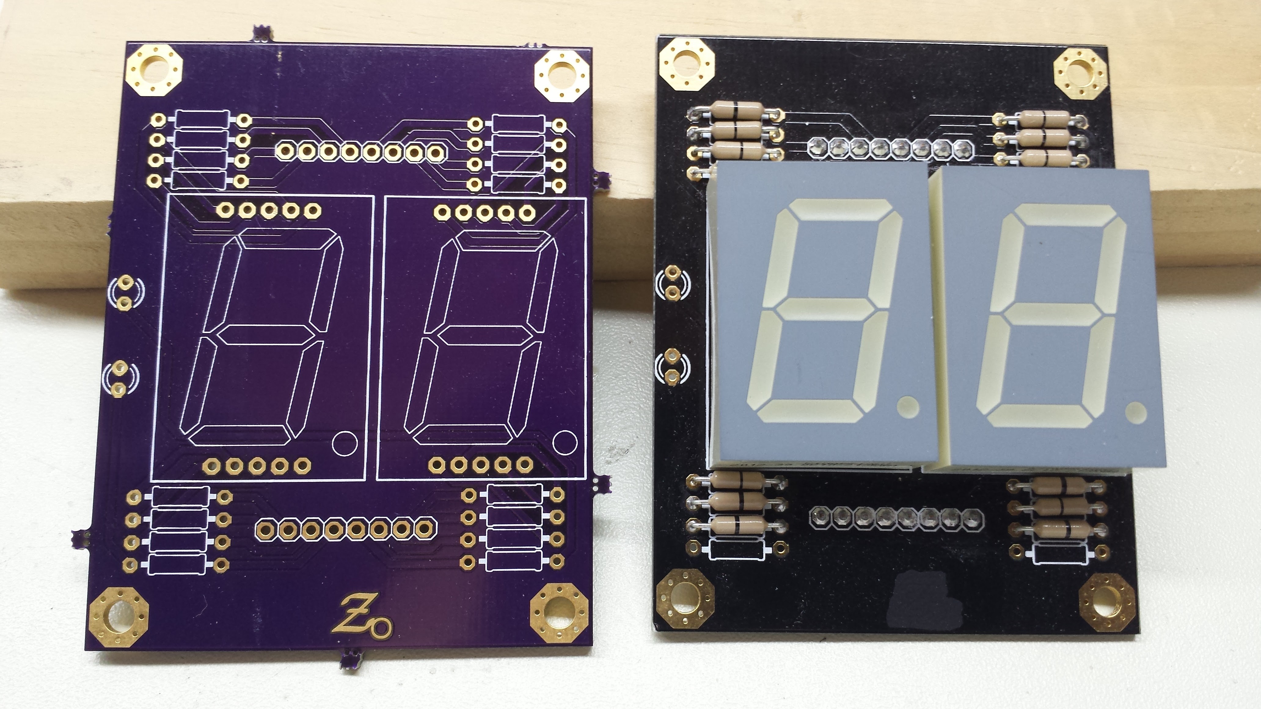
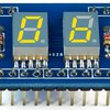
- Display Board (design files, project log, OSH Park): carries (2) 7-segment displays, forming 1/3 of the clock face.
- TCXO Timebase: Not a DDL-series board, but used for the Diode Clock to provide 1 PPS timekeeping pulse and 24H cycling test.
- DDL Demo Board (datasheet, design files, project log, OSH Park) Not a DDL-series board. I think this is the simplest DDL-style sequential logic circuit you can build. Stores a single bit (0 or 1) of your choice.
Background
When I was a kid, my parents bought...
Read more »


 Nick Sayer
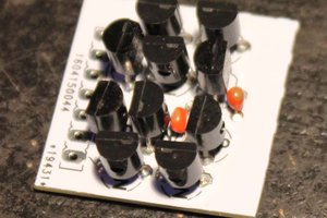
 Yann Guidon / YGDES
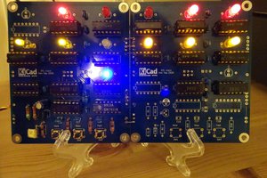
 Ken Yap
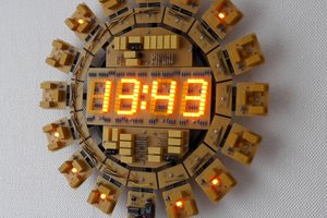
 Dave Gönner
Awwww damn, this is way beyond cool! A thing of beauty and a joy for ever. Clearly a lot of good work put into it. And all these blinkenlights... 10/10, would gefingerpoken und mittengrabben. Congrats!