 Nicolò
This project aims to have a fully working thermostat that anyone can use and also have some special IOT capabilities.
This is a quick list of the features I need:
- Toggle On and Off a relay to manage the "TA" contacts on italians boilers. (The TA contact is the heater pump contact)
- Timing functionalities, create different setpoint and schedule them.
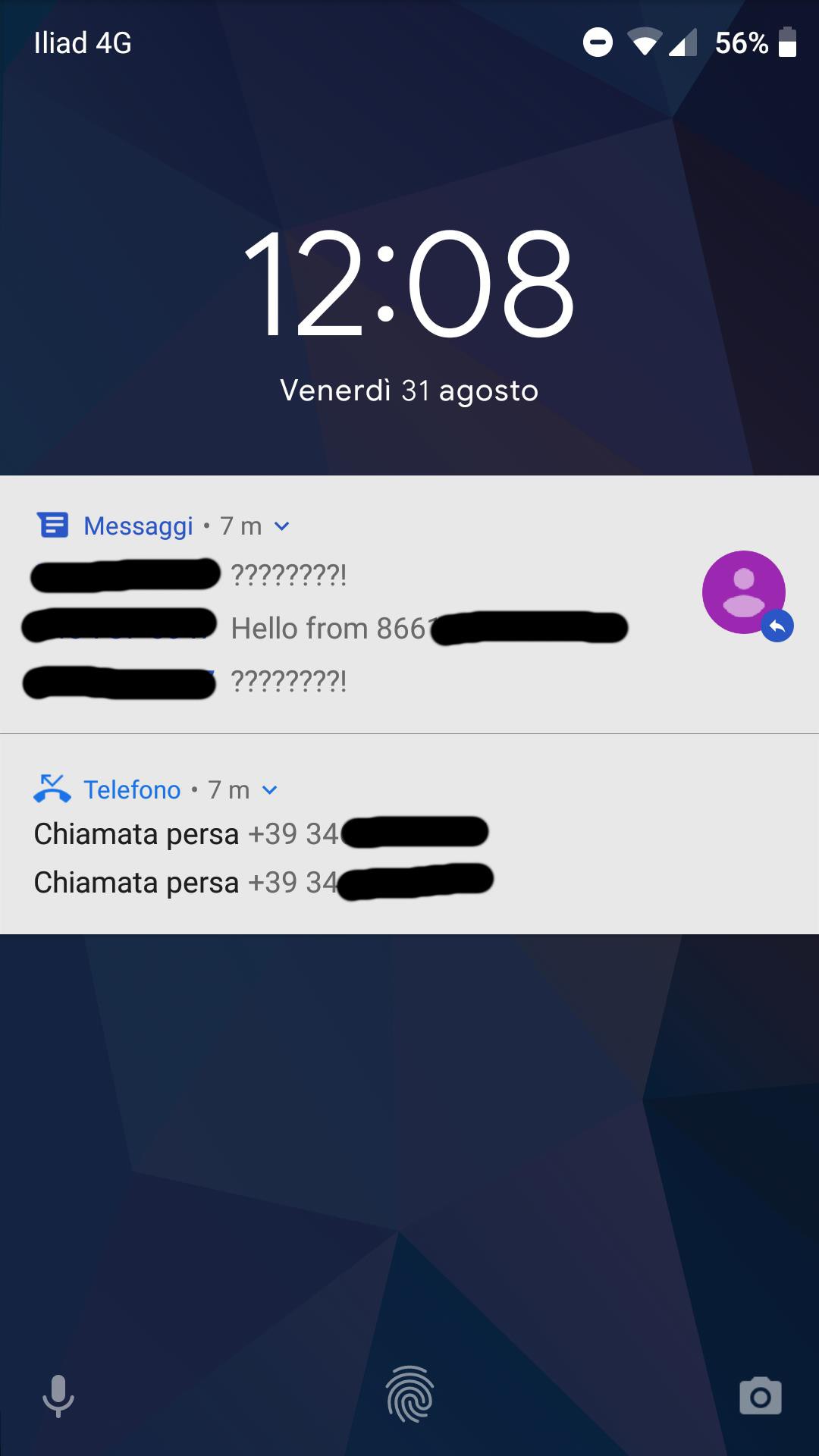
- Been able to turn ON and OFF the heat remotely. Via GSM or Internet. (In Italy we still have GSM/GPRS)
- Display the current enviroment data: Temereature and Moisture.
- Log enviroment data?
- Maybe, "make me a beer"? (No I'm not joking)
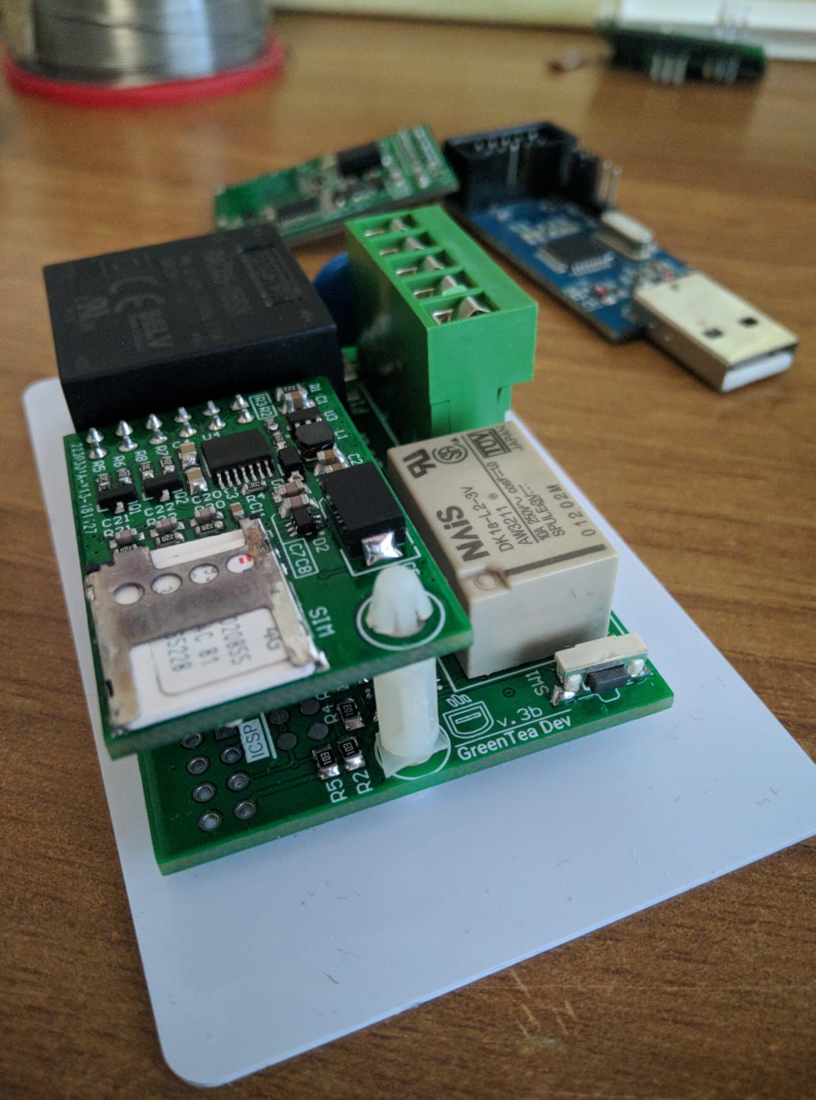
Right now The project is divided into three main parts:
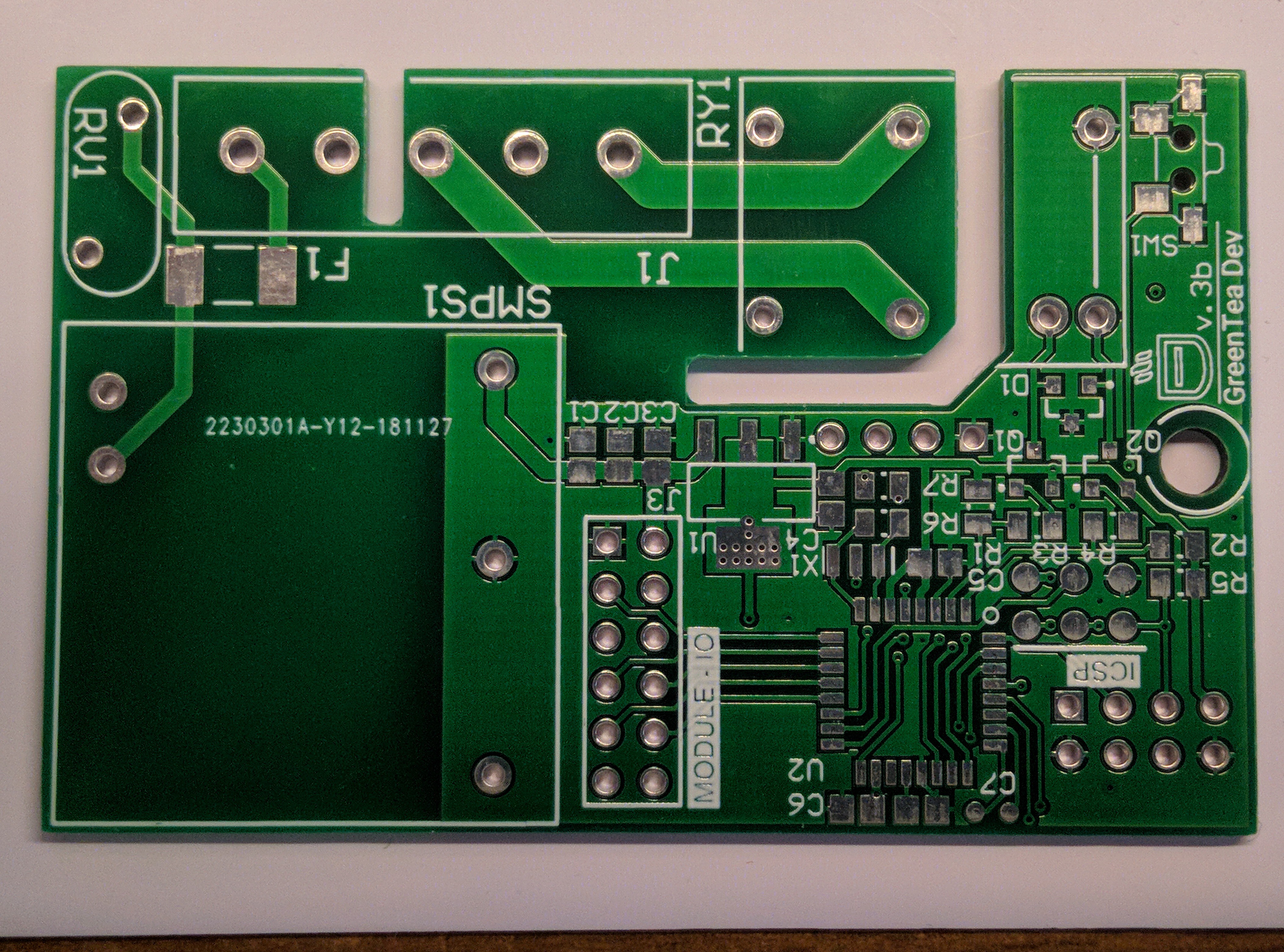
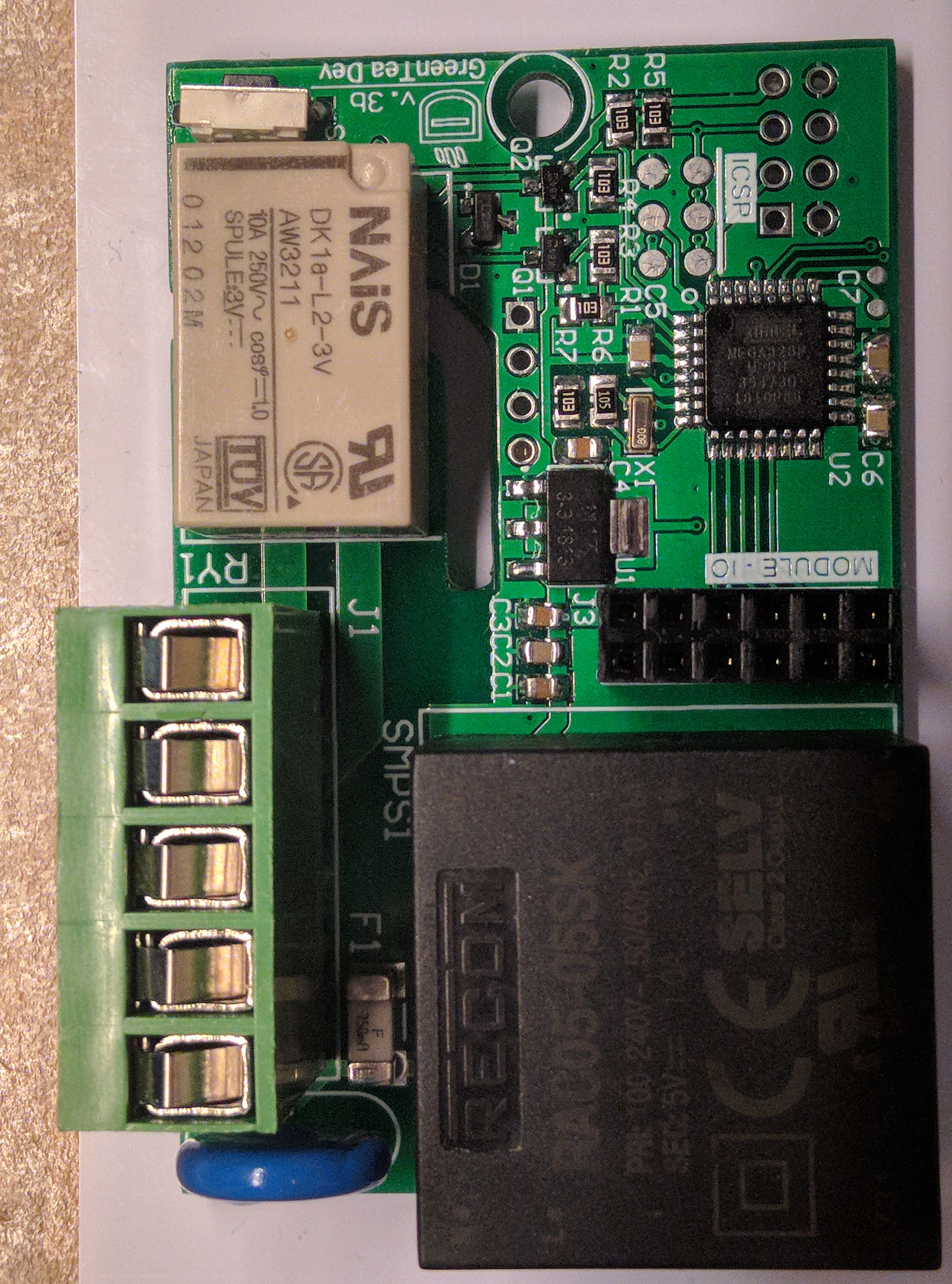
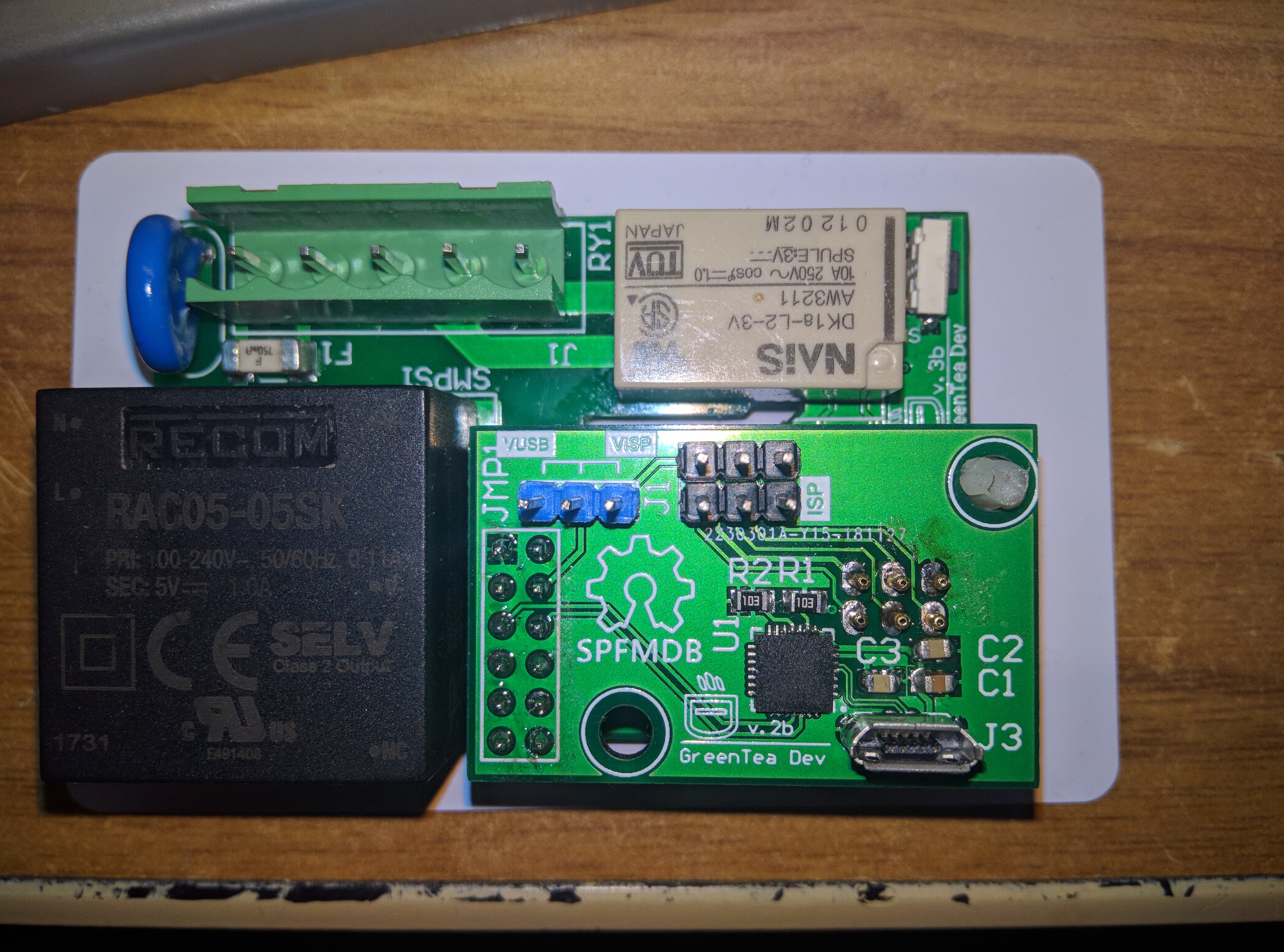
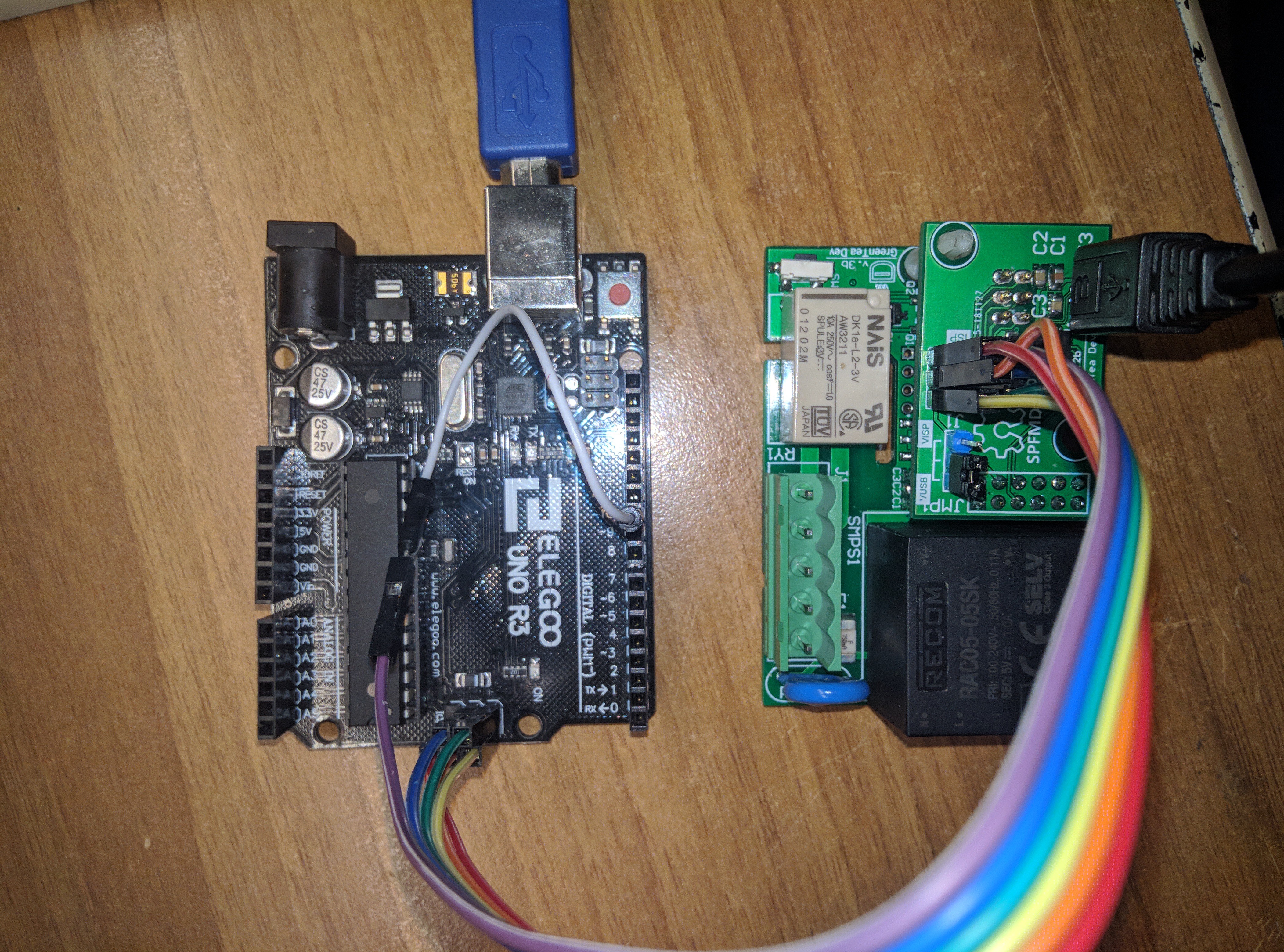
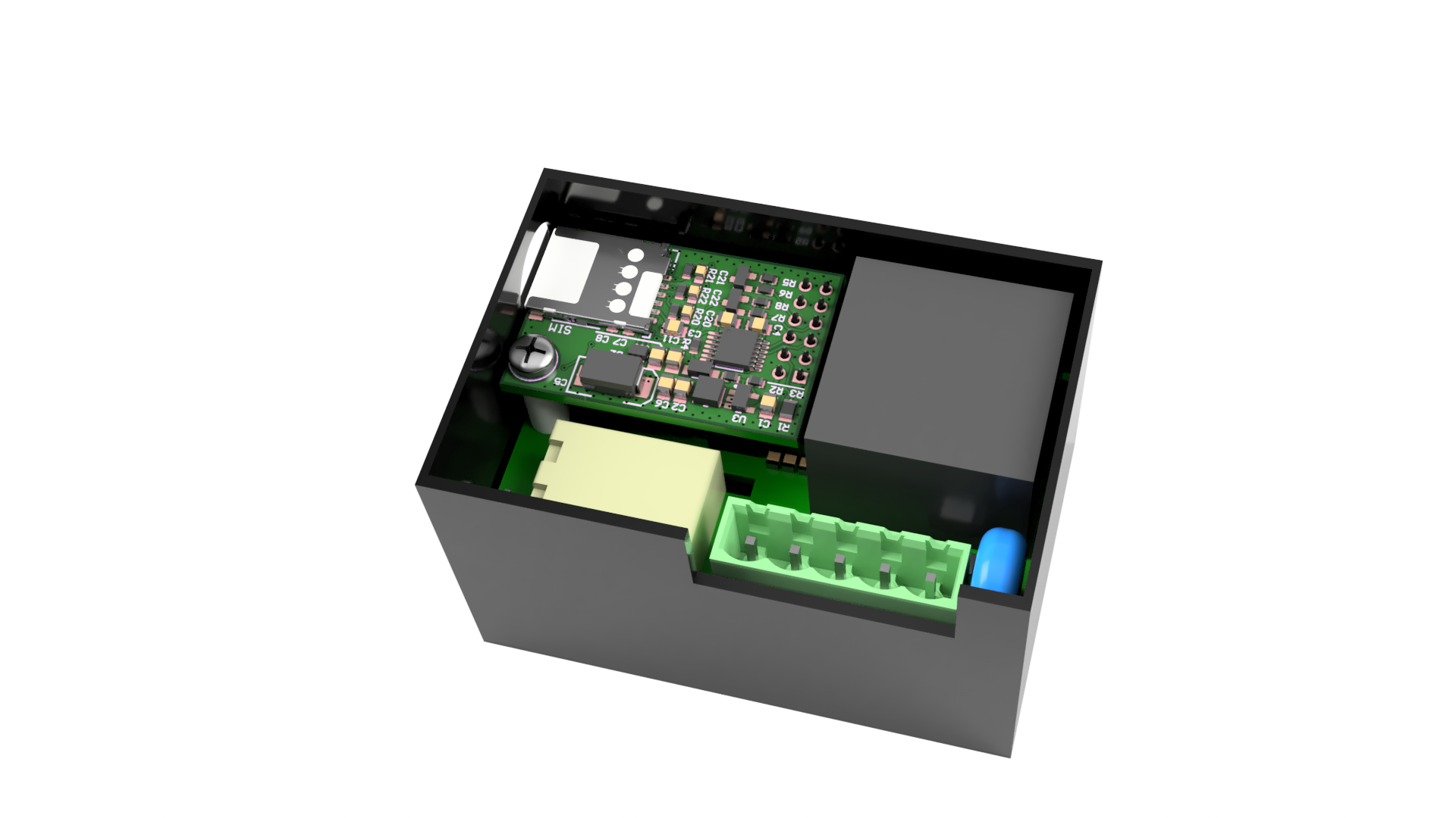
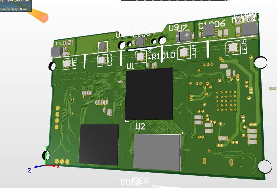
- The baseboard: it have the mains supply and the AC contact of the relay. (NC and NO)
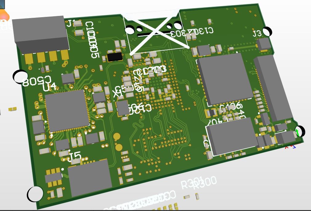
It have the "slave" microprocessor that manage all the IO - The expansion boards: A board that can be connected to the baseboard. This can be used to add mroe functions to the baseboard. Right now I'm working on the GSM module.
- The front. It have the main processor, it have the power juice to run all the stuff I need. It has a ring of RGB led and the EPD display. (Looks like that nowdays RGBs are a must)
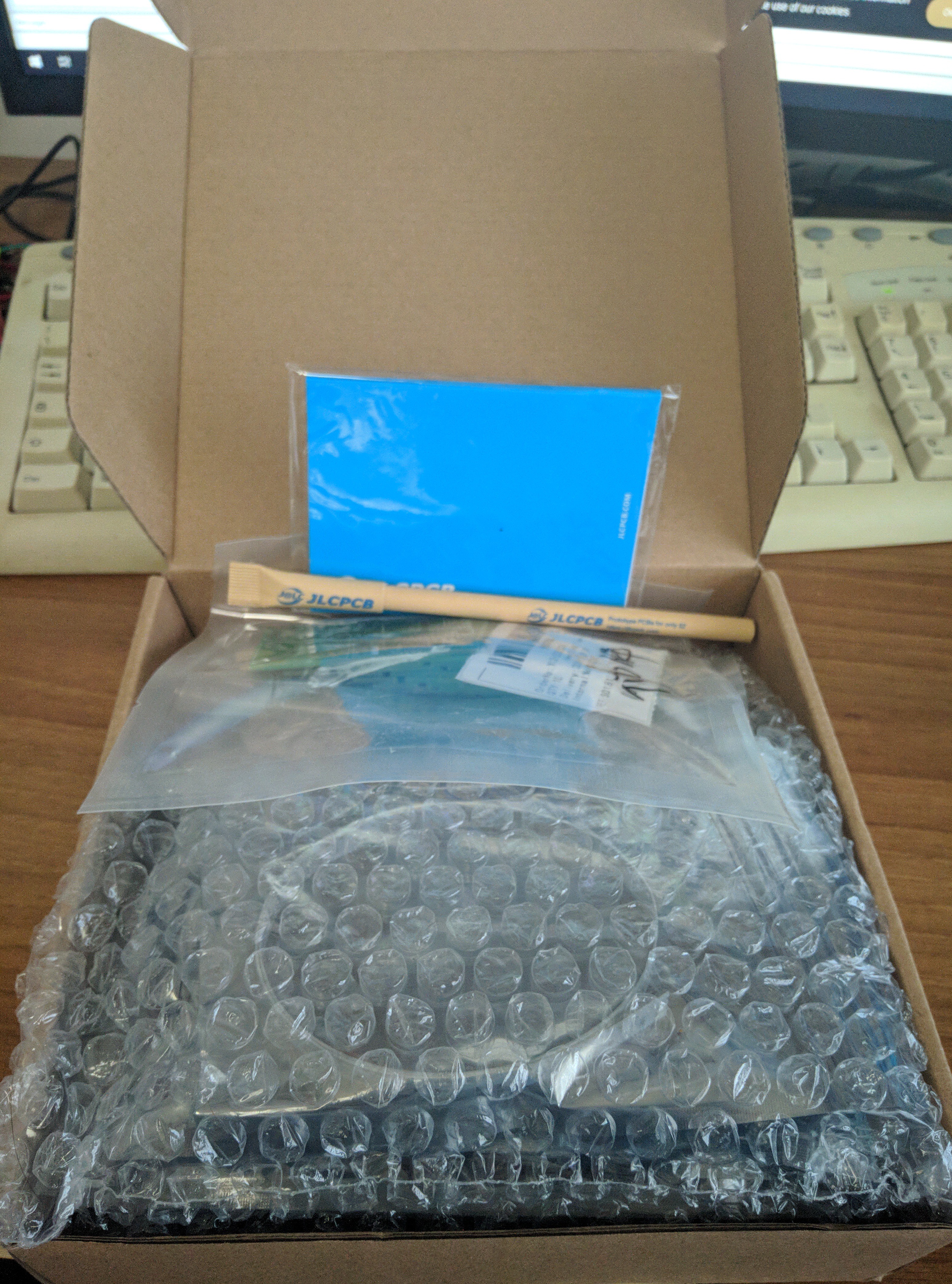
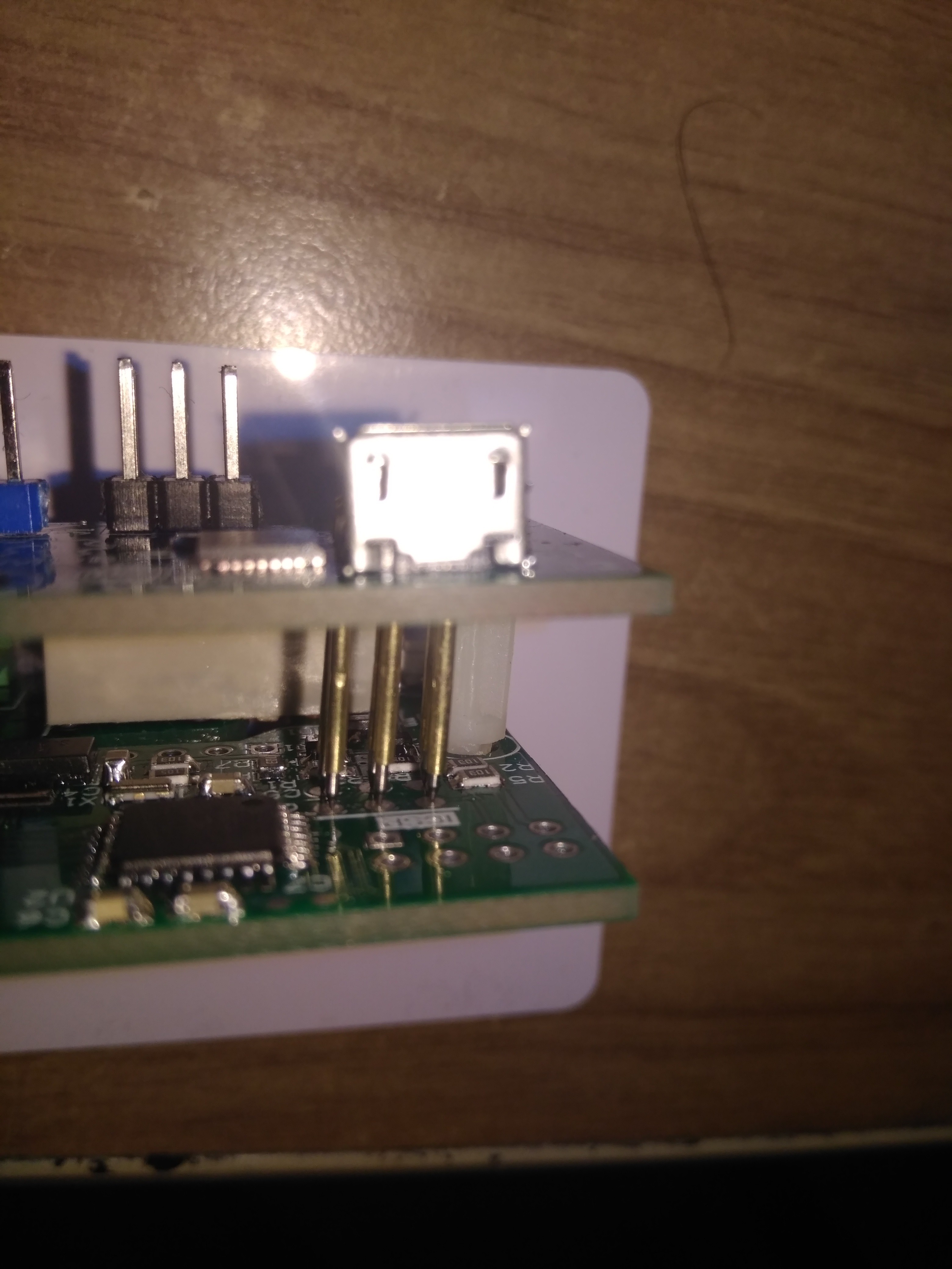

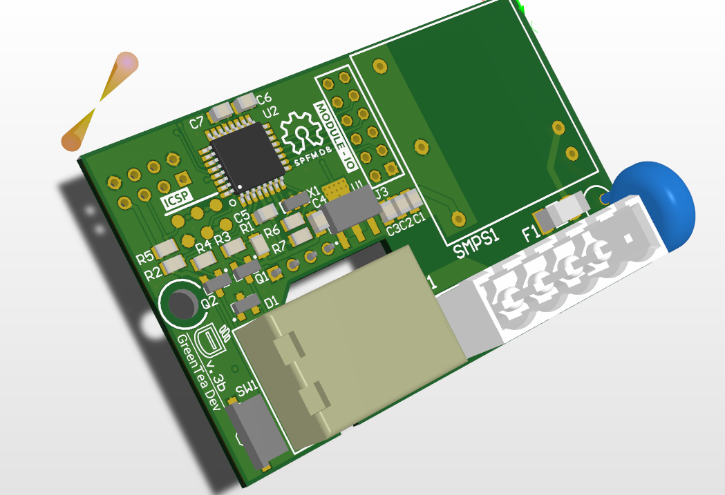 Also the programmer has been modified, now it have a built in USB to serial converter in this way I can program the Atmega with both the bootlaoder and the firmware itself.
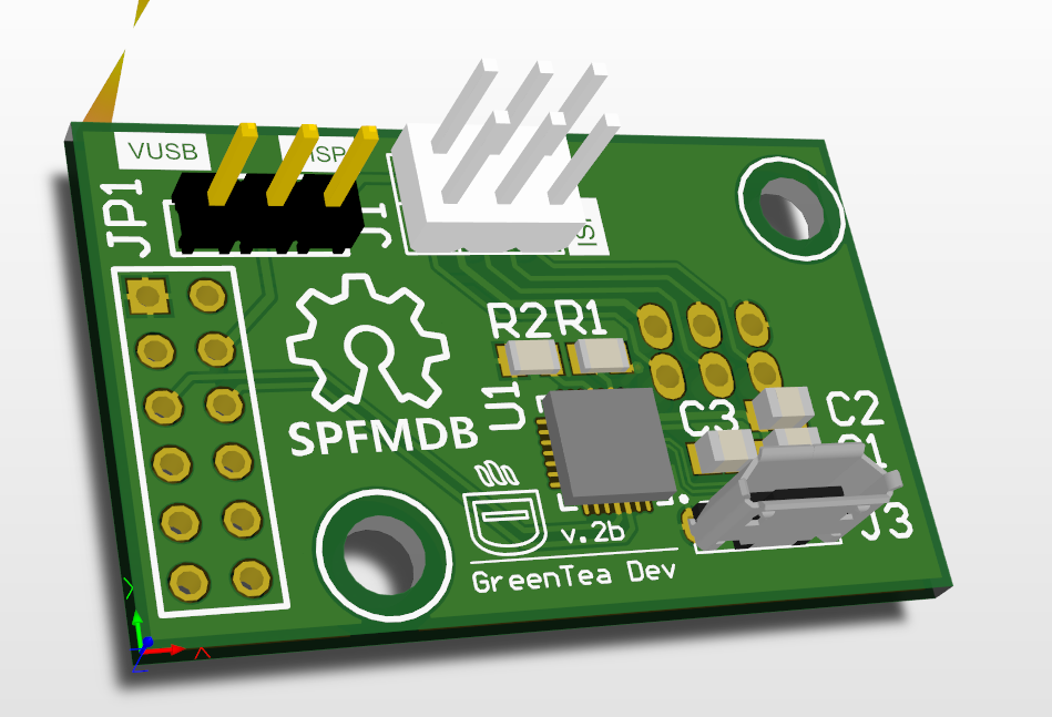 The board have a jumper to select the voltage source in this way I can use the 3V3 regulator inside the CP2102 or the one that is inside the ISP programmer.
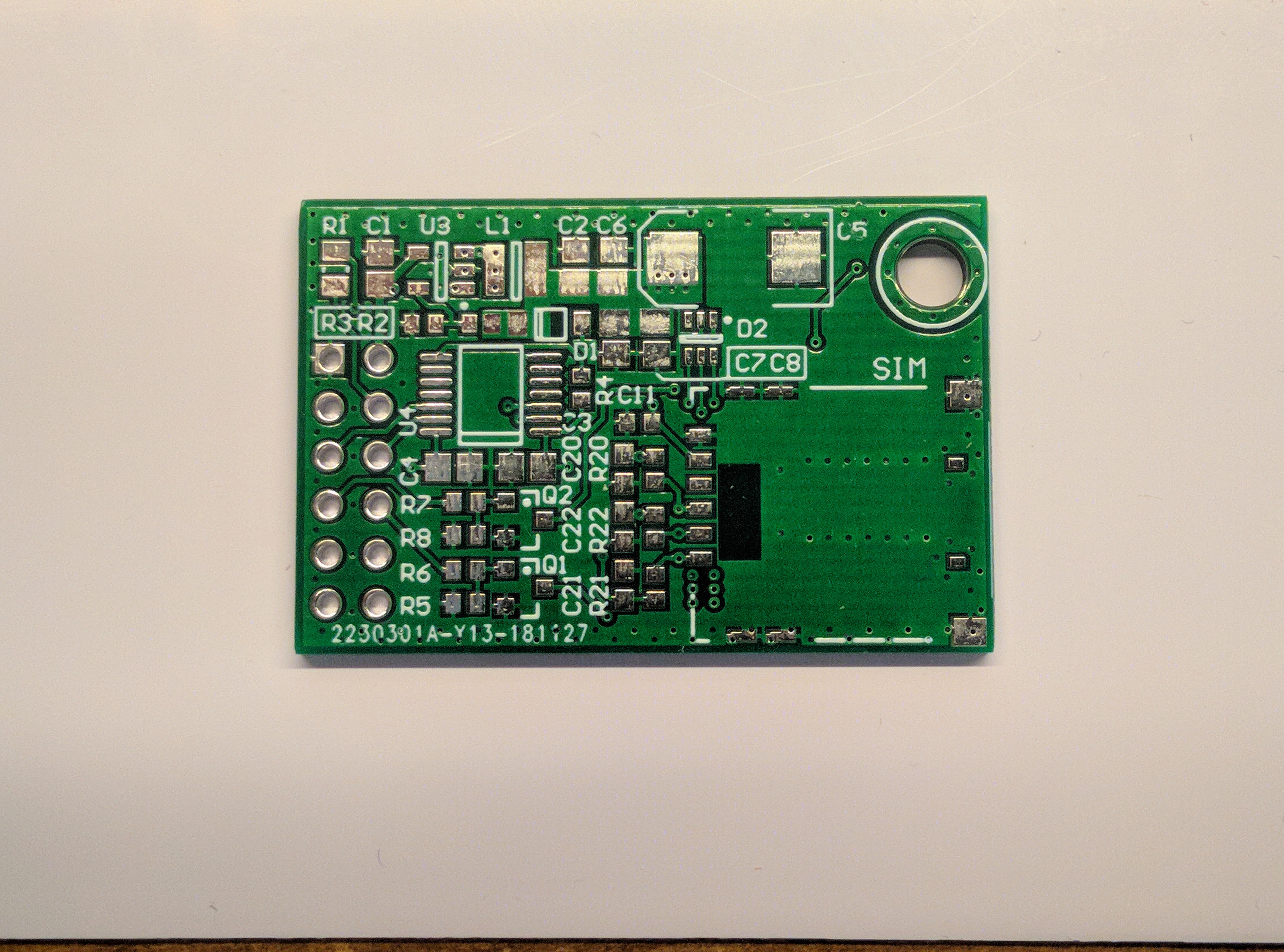
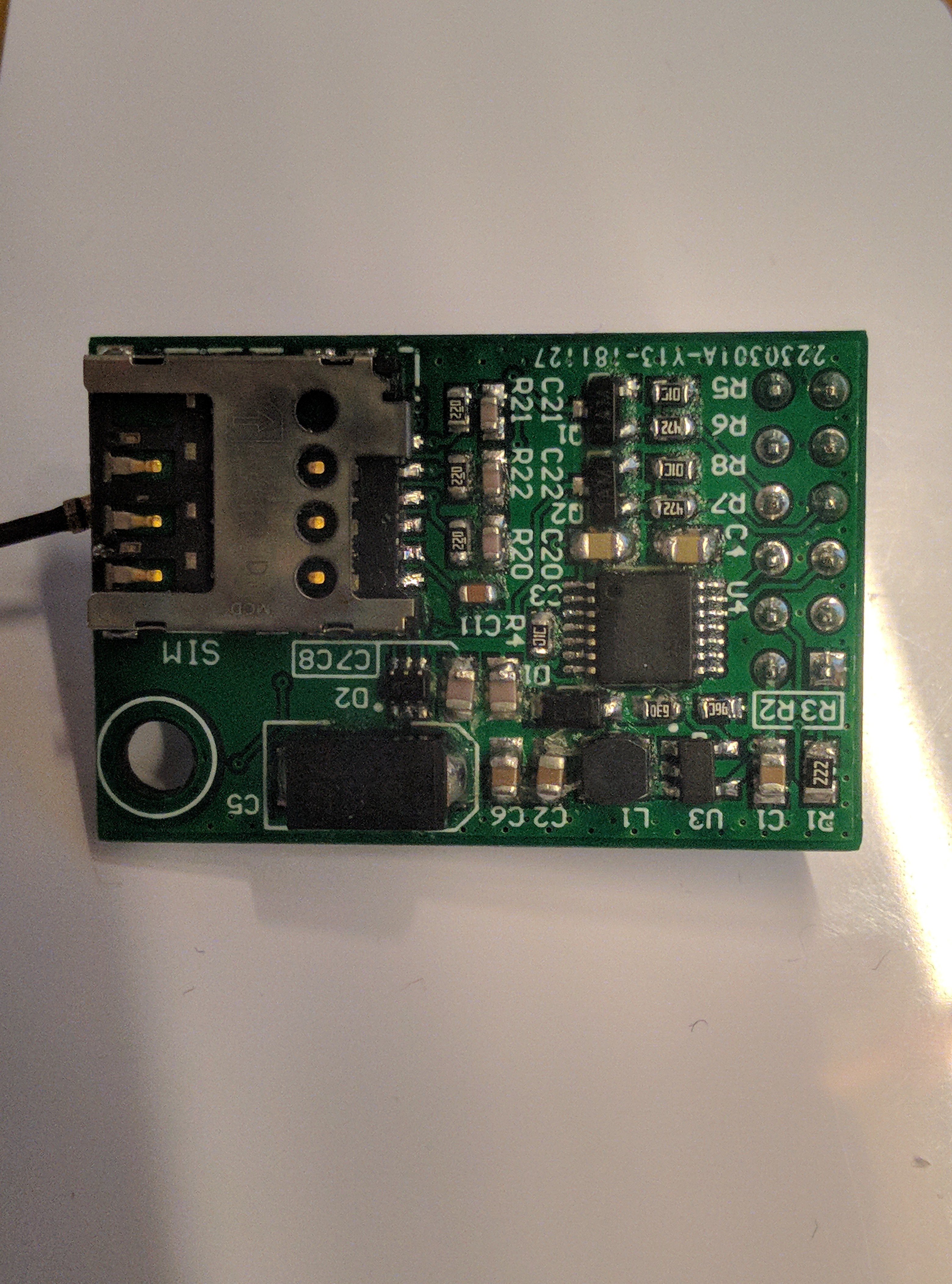
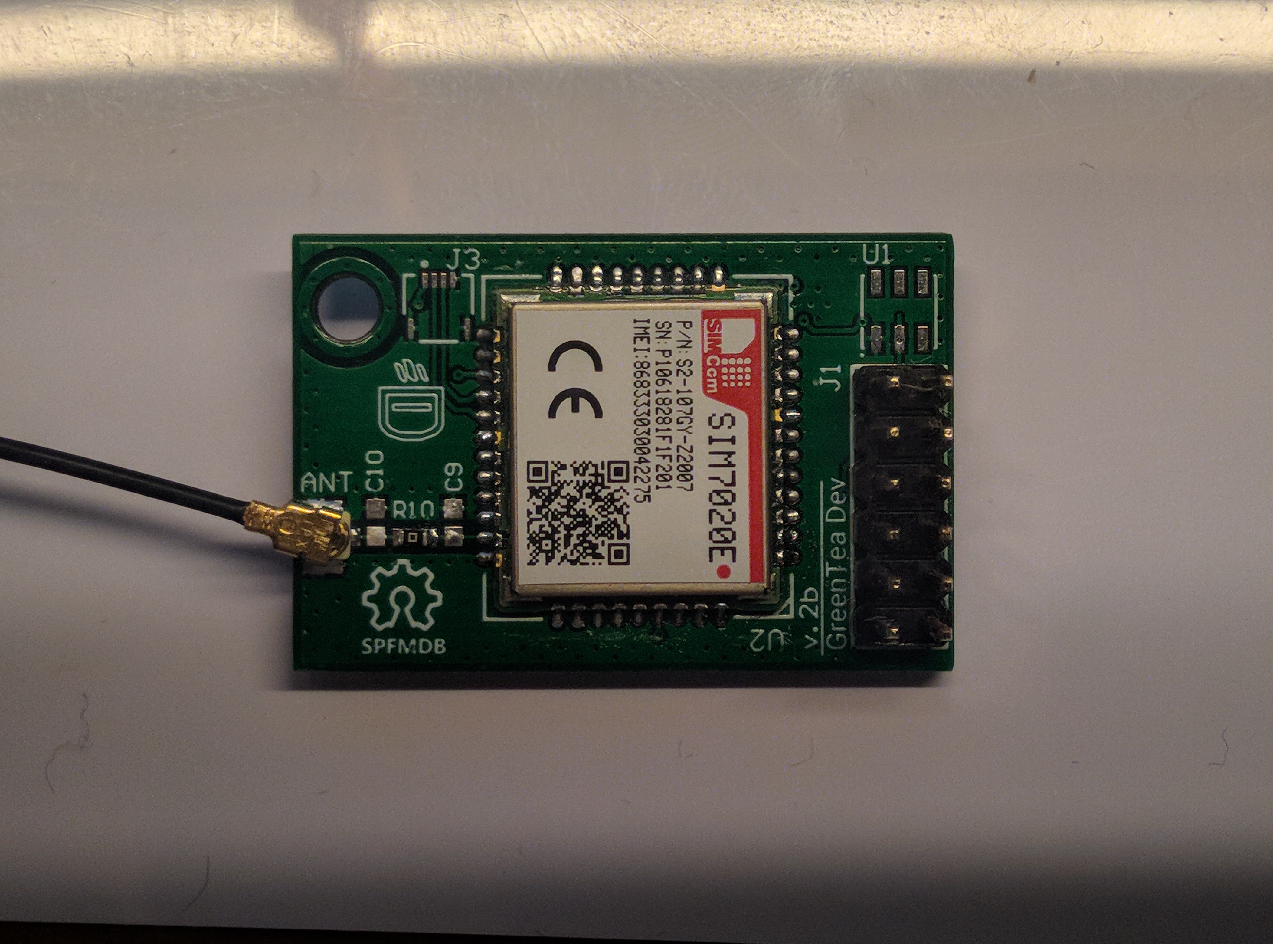
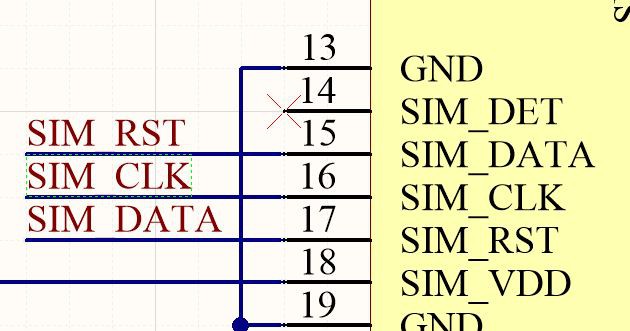
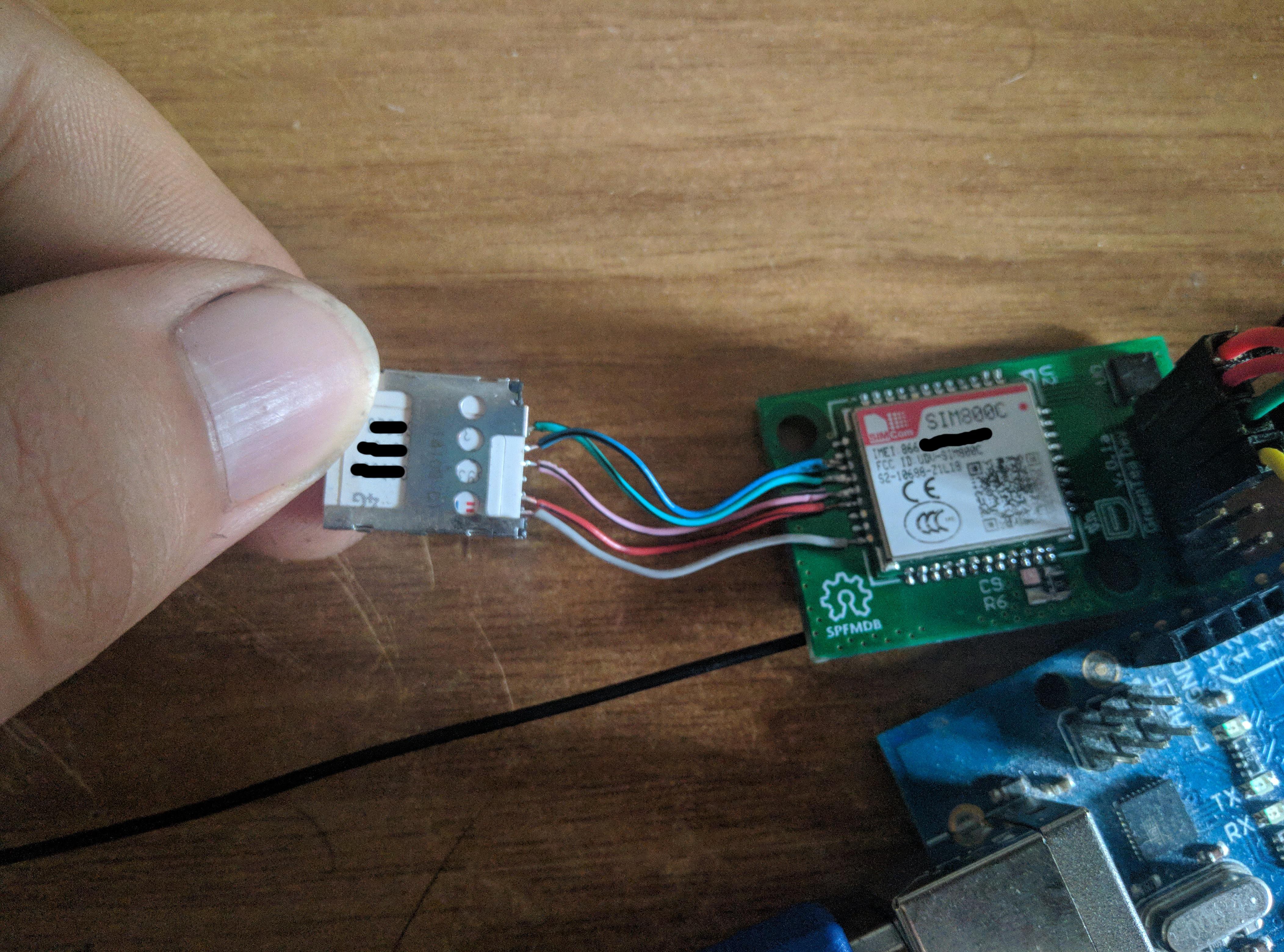
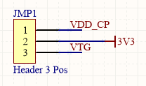 I have also reworked the SIM module, now it should work without problems. I have added more vias to shield it and with the tips from Raúl I created this layout:
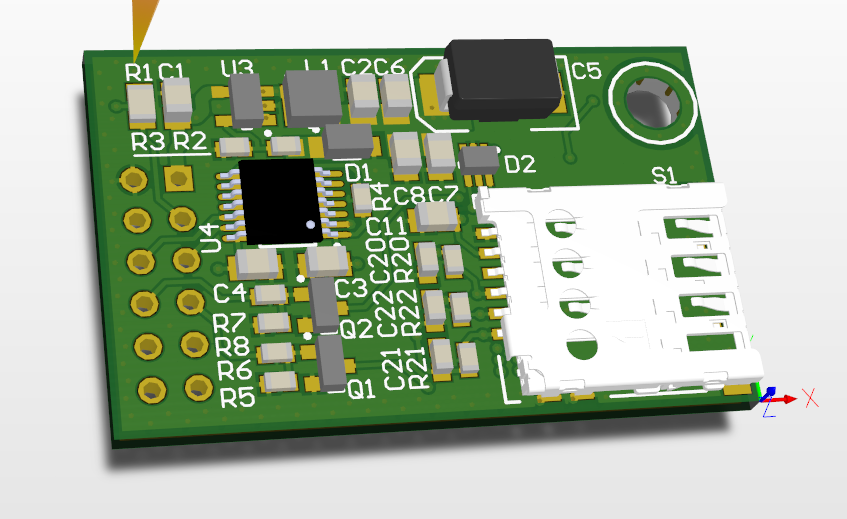 This one have all the necessary components for the SIM holder, and the PI network on the antenna. The big step was to replace the 0805 components with 0603. (With the exceptions of some
 OzQube
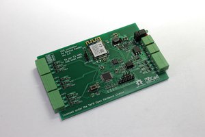
 Michel Racic
 Jared
Jared