 Christoph Tack
Requirements
- Compact
- Powered by ubiquitous 18650 cells
- Option to connect Li-Po instead of 18650
- Including Li-Ion charger
- Charging while load is connected
- Charging options:
- USB
- 5V solar panel: up to 8V input should be accepted.
- Route VIN through : 5V output when powered by 5V
- Power input connector:
- USB micro
- JST-PH
- Outputs
- Primary output : 3V3/1A output
- Secondary output : 1.2V to 12V output, controlled by trimpot
- Efficient power conversion
- Low standby current
- Option to turn off outputs remotely to save power
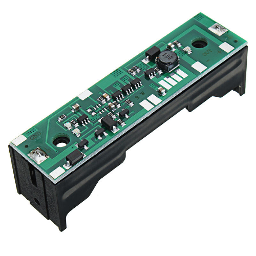
COTS
Why make it when you can buy it?
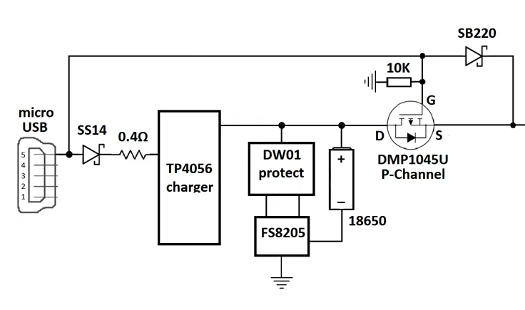
- TP4056, can be directly connected to solar charger
- 3V3/1A created by 3 parallel LDO (77µA total quiescent current)
- 5V/1.7A boost converter (260µA quiescent current). There's no way to turn the boost converter off.
- Not suitable to charge and discharge simultaneously.
- Quite big
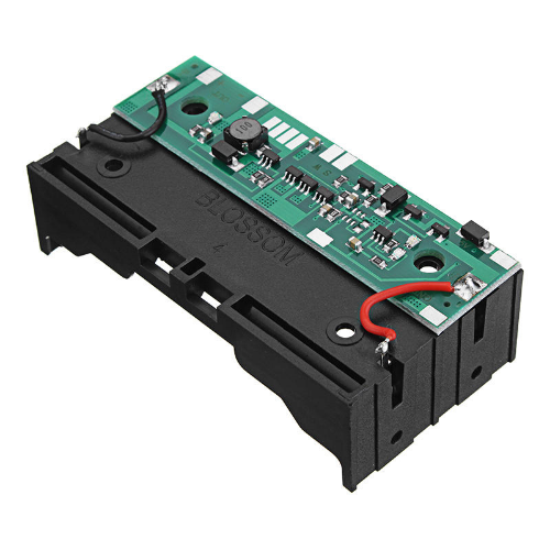
This one from AliExpress has only a 5V booster.
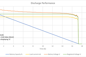
How much current is needed?
The original idea was to build a 3V3/2A supply. But is that a good idea? How many battery powered applications need a regulated 3V3 at 2A? Sure we can build it, but it will be running at much lower currents for most of the times. The efficiency at lower currents will be much lower. The cost will be higher because of the bigger inductor and more expensive switcher.
1A will be enough for most applications, including the #easy-alarm-clock for which it has originally been designed.
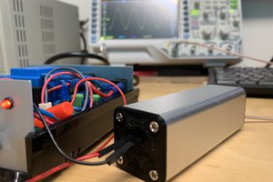
Implementation
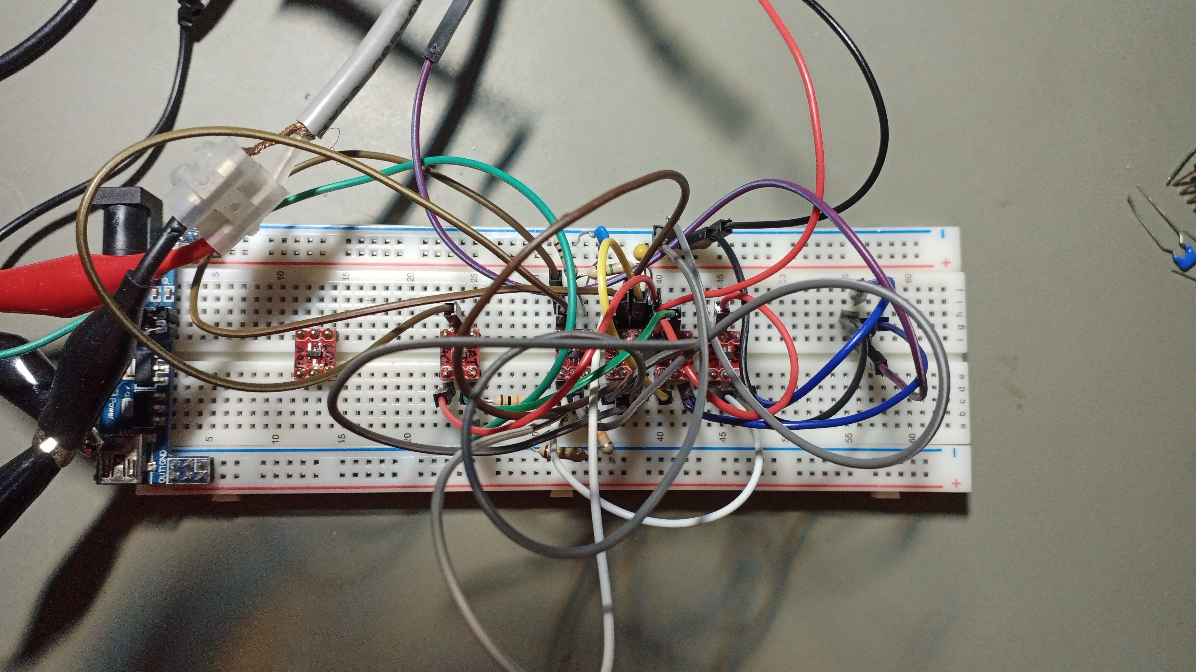
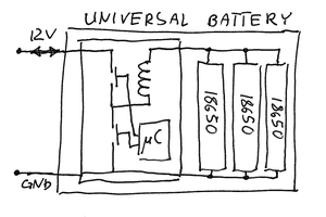
The original plan was to design a single PCB, but I expected to use this project too little. Instead it will be converted to a modular design consisting of four small SMD-modules:
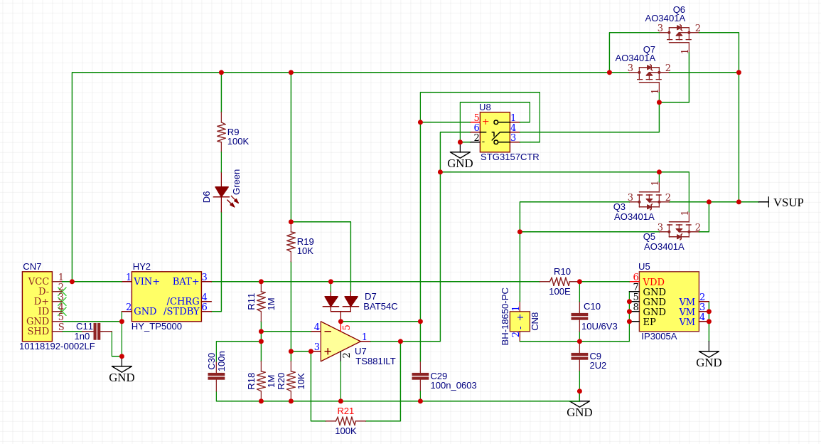
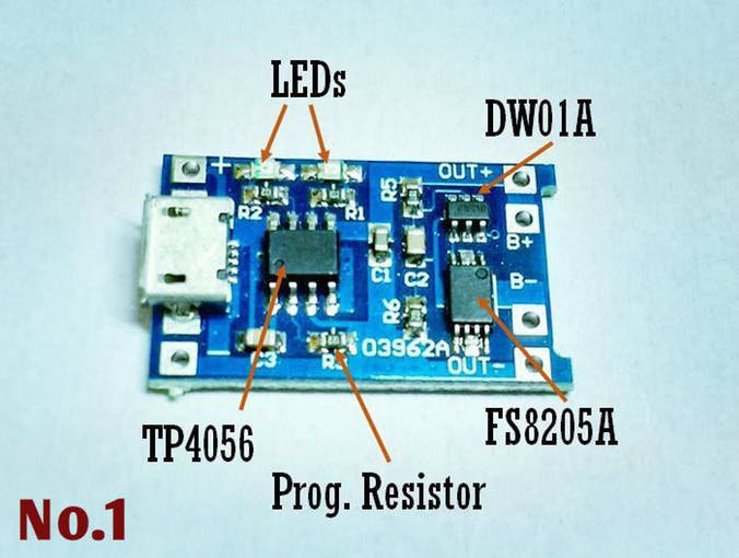
- Battery charger : will be existing TP5000 module (cheap, also charges LiFePO4, wide input voltage range)
- Battery management : existing modules based on the DW01A. Wide range of current output ratings available (by paralleling FS8205A mosfets)
- Buck regulator based on AP3429A (obsolete?)
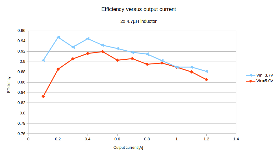
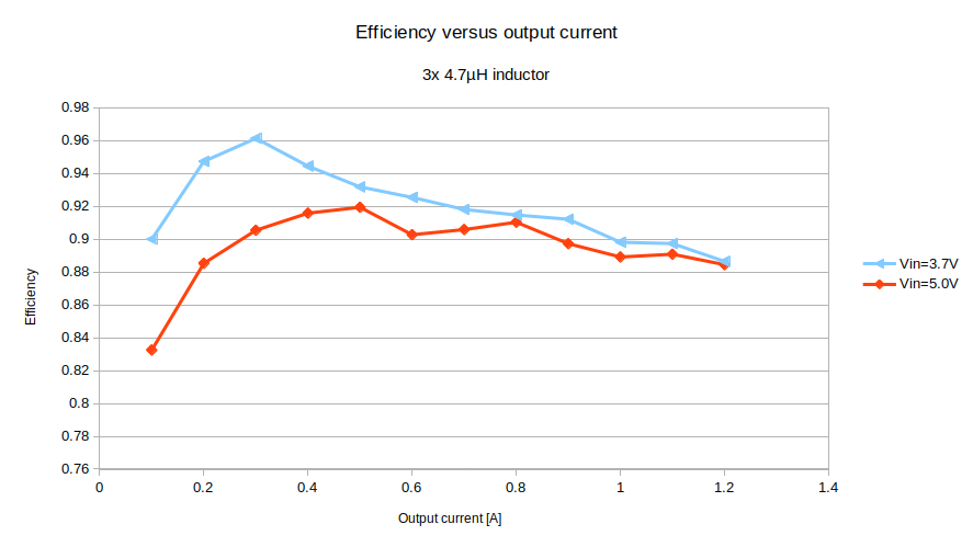
- Buck/boost (sepic) regulator based on LM2731X


 George
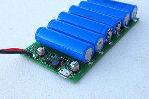
 Patrick Van Oosterwijck
This is really useful information i must say that this is really nice thanks for sharing with us. https://www.adpworkforce-now.com/