 Mitsuru Yamada
Detail
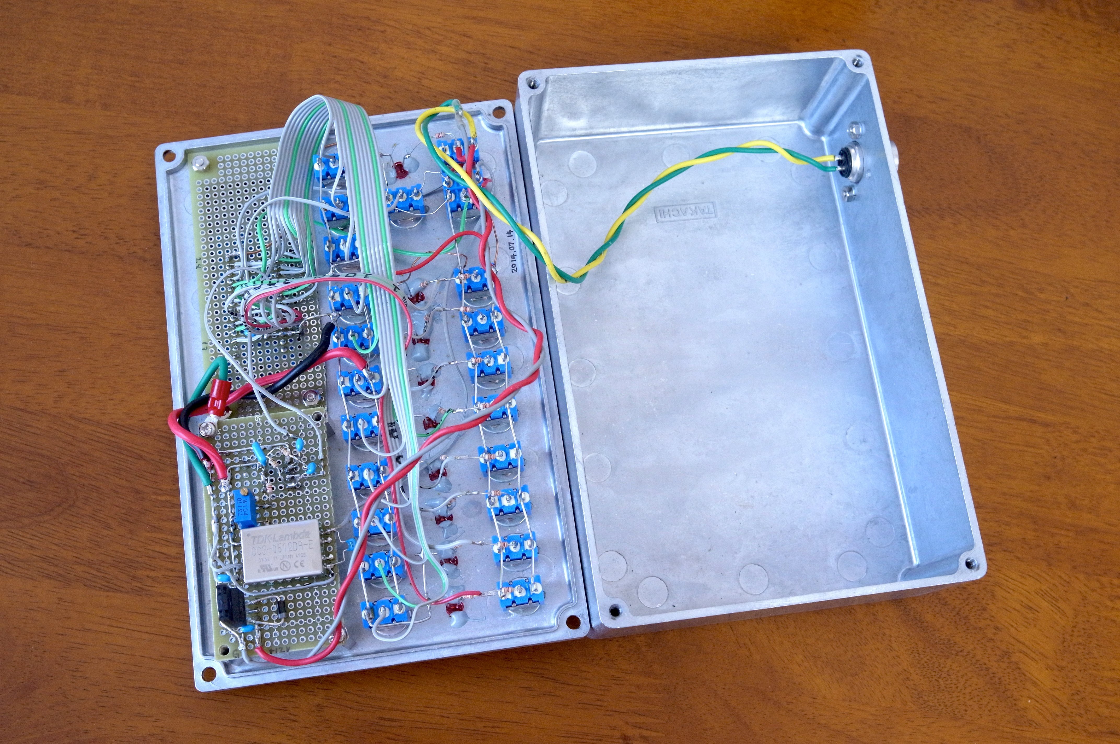
As shown in the schematic, the address toggle switches, the data switches, and the LEDs are connected to the PROM device directly. Vpp +24V is supplied by DC/DC converter. Since the PGM signal need 50ms single pulse, a one-shot multi vibrator NE555 is used. For a reading mode, Vpp is applied +5V and an output enable of the PROM is set active. For a programming mode, Vpp is applied +24V and an output enable is set inactive. If you press the write switch here, the 50 ms programming pulse is generated, then the data value will be written to the PROM. The following is a photo of the internal structure.
Result
When the erased PROM is read in reading mode, all the bits are correctly high. In the program mode, set the address and data with switches and operate the write switch to program the data. To program is to make the bits low level. When the programming is done, you can check the written values again in reading mode.
As above, it can be said that this programmer works correctly. However, depending on the type of PROM, switching between a reading mode and a program mode while the power-on state could destroy the device. So, the mode switching need to do in power-off state.
If I tried manually programming 2 kbytes of data, it took about 5 hours. I also needed a lot of concentration so that I wouldn't make a mistake to set binary values by toggle switches byte by byte. This is a tough, but the basics of PROM behavior are well understood.
Reference: MM2716E 16,384-Bit(2048 x 8)UV Erasable PROM, National Semiconductor (datasheet)
Related articles:
Homemade Floating Point Interpreter for 6502
PERSEUS-8 homemade 6502 computer
https://hackaday.io/project/175923-rom-module-for-6502-standalone-computer
https://hackaday.io/project/175893-6502-computer-runs-calculator
https://hackaday.io/project/175866-6502-standalone-computer
Video:


 Justin R.
 Scott
Scott
 Marcrbarker
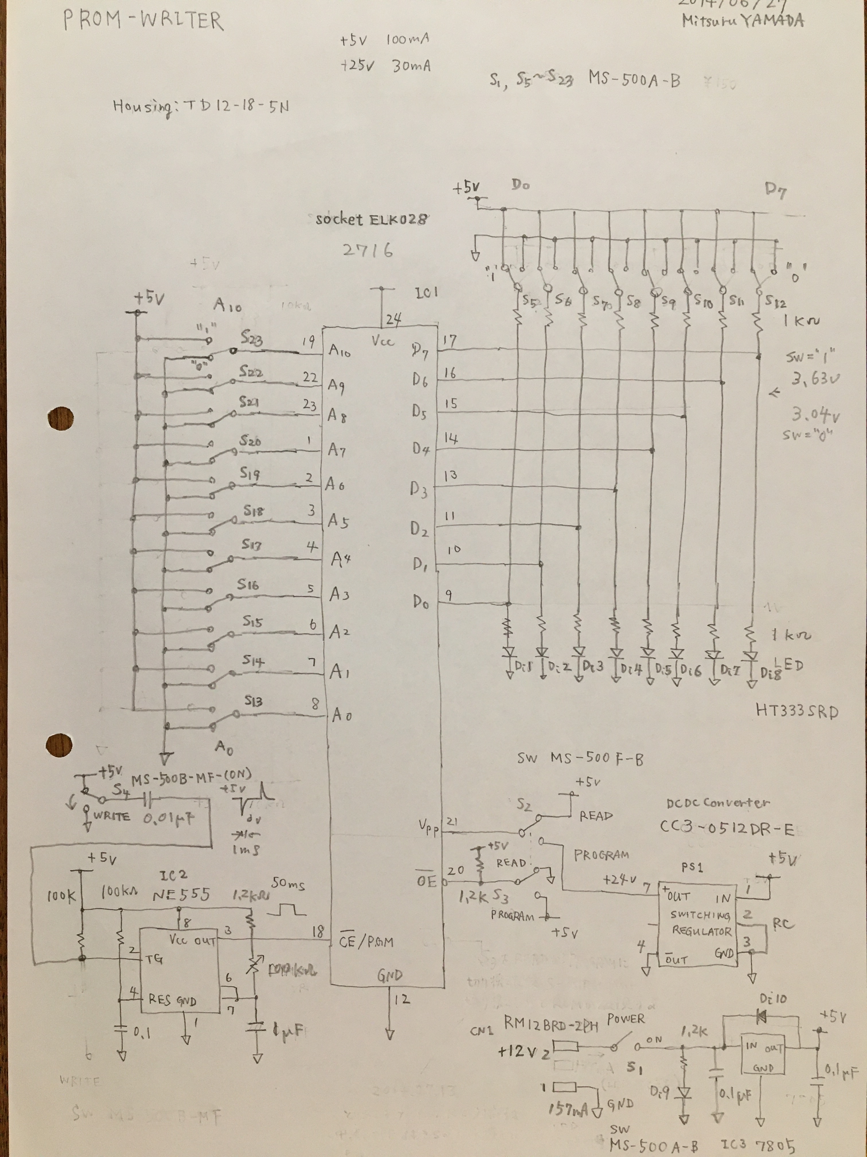
>If I tried manually programming 2 kbytes of data, it took about 5 hours. I also needed a lot of concentration so that I wouldn't make a mistake to set binary values by toggle switches byte by byte. This is a tough, but the basics of PROM behavior are well understood.
Wow, respect! 👍 I would probably make a mistake before reaching the 6th byte. One advantage of your programmer is that it can handle 25V parts, which my programmer can't. The newer models from that series can't even do 21V parts any more so I'm hanging on to my model.