 Hulk
HulkIt's been a while, the Autobots have appeared on the silver screen. Finally they are returning to the big screen in their upcoming Transformers movie "Rise of the Beasts".
This inspired me in making a PCB Badge to complement my enthusiasm and love towards the Autobots.
In this tutorial, I am going to show you guys how to design this "Transformers PCB Badge" and how to solder the components to it.
Components Required

For this tutorial you need:
- 1 x 555 Timer IC
- 1 x 47KΩ Resistor
- 1 x 220Ω Resistor
- 1 x BC548 NPN Transistor
- 1 x 33µF Capacitor, and
- 1 x Few Blue LEDs
Quick Recap
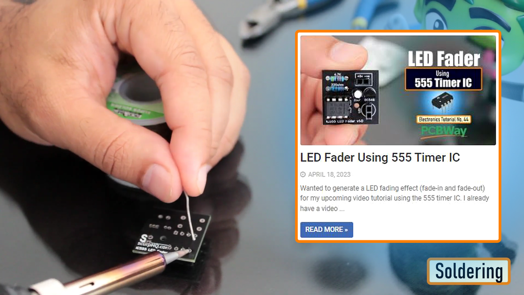
In my last tutorial I created a "IC555 Led Fader Module" and explained how the circuit works. In this tutorial, I am going to use the same LED fader circuit to create a fading effect for the eyes of the badge.
So before going ahead, lets do a quick recap and find out how the LED fader circuit works with the help of an animation.
Circuit Diagram

The heart of this circuit is the 555 timer IC.
Pin No.1 of the IC is connected to GND.
By connecting Pin 2 and 6 of the 555 timer IC, we put the IC in astable mode. In astable mode, the 555 timer IC acts as an oscillator (re-triggering itself) generating square waves [PWM Signals] from the output Pin no. 3.
3 other components connect to this junction.
1st one is the 33µF capacitor. The positive pin of the capacitor connects to the junction and the negative pin is connected to the GND.
2nd one is the 47KΩ resistor. One of its legs connects to the junction and the other leg connects to the Output pin, Pin No.3 of the IC.
3rd one is the Base of the BC548 NPN transistor. The collector of the transistor along with Pin 8 and 4 of the IC connects to the +ve terminal. of the battery. The LED along with its current limiting resistor is connected to the Emitter of the transistor.
That's+-
How The Circuit Works

- When Pin 2 of the IC detects voltage LESS than 1/3rd of the supply voltage, it turns ON the output on Pin 3.
- And, when Pin 6 detects voltage MORE than 2/3rds of the supply voltage, it turns OFF the output.

This is how the trigger pin (Pin2) and the
threshold pin (Pin6) of the 555 timer IC sense voltages and controls the output at Pin 3.

- The Capacitor attached to the circuit will be in a discharged state immediately after firing up the circuit.
- So, the voltage at Pin 2 will be 0v which is less than 1/3rds of the supply voltage, this will turn ON the output on Pin 3.
- Since Pin 3 is looped back to Pin 2, it will start charging the Capacitor via the 47KΩ resistor.
- At the same time the base current of the transistor also increases causing the LED to slowly "fade-in".
- Once the voltage across the capacitor crosses 2/3rds of the supply voltage, Pin 6 turns OFF the output.
- This causes the capacitor to slowly discharge causing the base current to fall and hence the LED starts "fading-out".
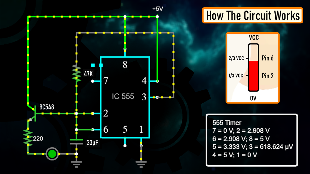
- Once the voltage across the capacitor falls below 1/3rd of the supply voltage, Pin 2 turns ON the output, and the above cycle continues.
You can hook up a multimeter to the circuit to measure the charging and discharging of the capacitor.
Designing The PCB
Sorting Out Images

To start the designing process, I need a transparent PNG image of the "Transformers Logo".
So I went online, and did an "image search" and downloaded a black-and-white images of the Transformers Logo.
Now, using the "Paint.Net" application I opened up the PNG file.
The image onscreen will be used for:
1. Creating the border outline of the badge
2. and also for creating the face on top of the top silk layer
To generate the "Border Outline" I need a DXF file.
Looking at the image, we can see that the image is split into multiple parts. If I load this to generate a DXF file it will generate multiple pieces of the PCB. And obviously that's not what I am after. So, I joined all the small pieces into a single image.
Generating DXF File
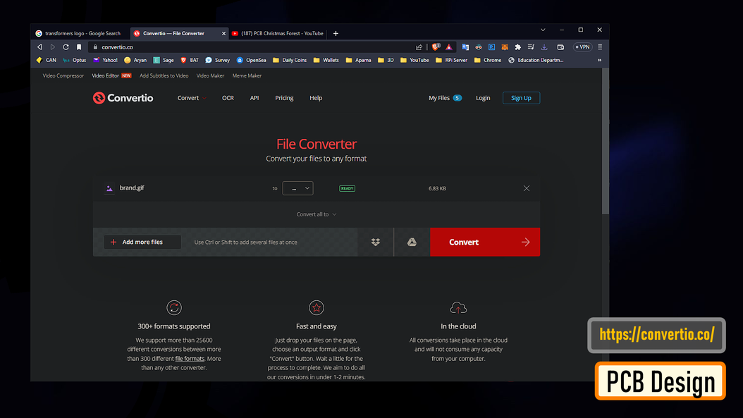
Then, I uploaded the images to "https://convertio.co/" to generate...
Read more »
 Lithium ION
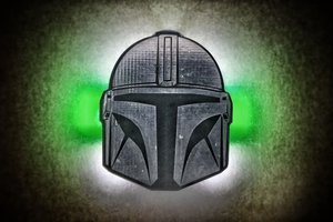
 Fabrizio
 Jithin Sanal
 ElectroBoy