Project Overview Video for Hackaday Prize 2023:
The End Result
The Plan
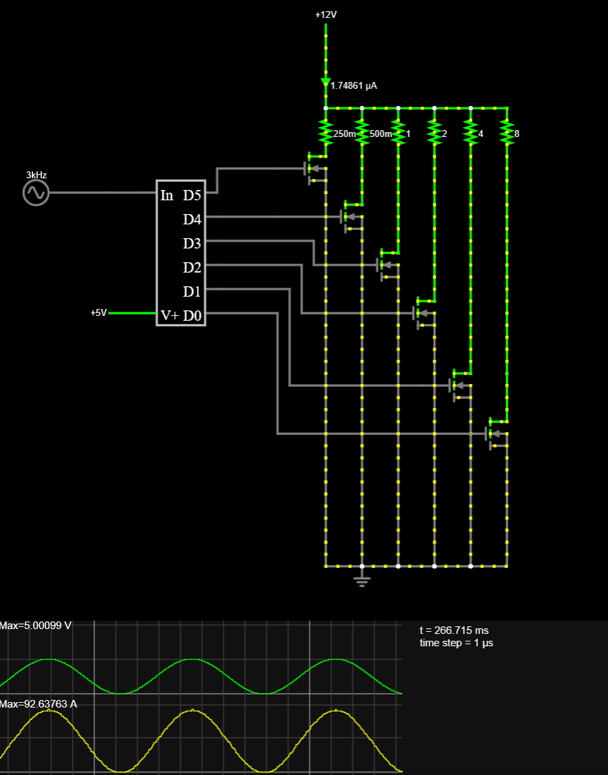
In principle it is simple: by connecting different combinations of binary value resistors in parallel, and assuming a constant input voltage, we can consume any arbitrary amount of current between just having the smallest resistor on and having all of them on. Implementing this gets much more complicated as current and pulse frequency rise.
For my power supply testing application, I've targeted the following specifications:
- Nominal 12.2V load input (3.3V-14.6V accepted)
- 750A (9,150W) for one hour continuously
- 1300A (15,860W) for 10 seconds
- 2700A (32,940W) for 100us pulses (100us on, 200us off, 33% duty cycle at 3.3kHz)
Taking into account resistor tolerances and variation over temperature, the following resistor values were chosen to meet these specifications:
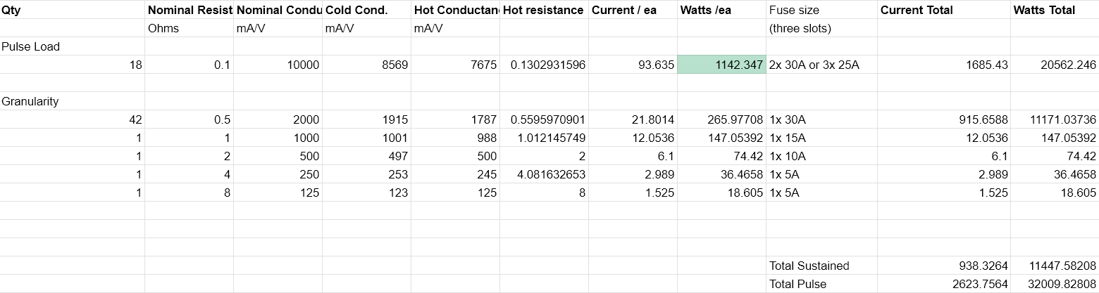
I'd initially planned on using mostly 1000W 0.25R resistors to make the bulk of the continuous load, however they doubled in price during design and so they are no longer cost effective.
Wanting a certain number of resistors switched in and out is a far cry from an actual implementation. How do you mount them? Wire them? Cool them? Control them? Prevent the switching FETs from getting damaged by the inductive spike on each turn-off? Nothing is ever quite as simple as it appears.
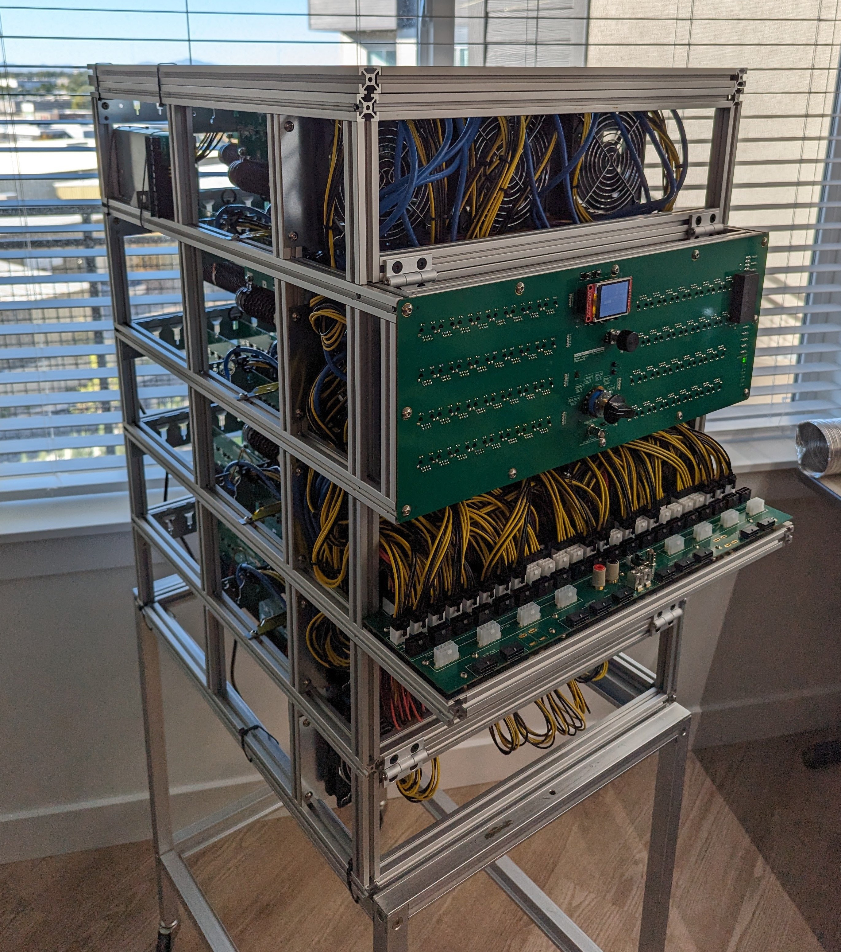
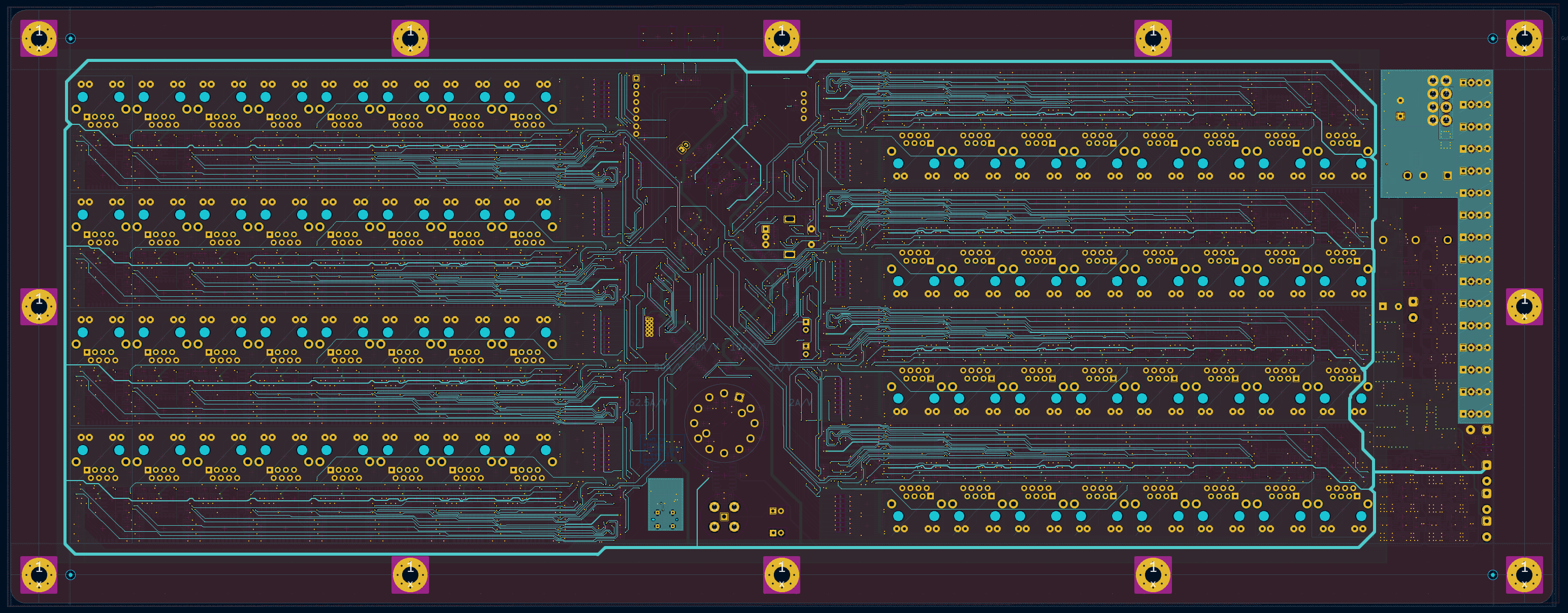
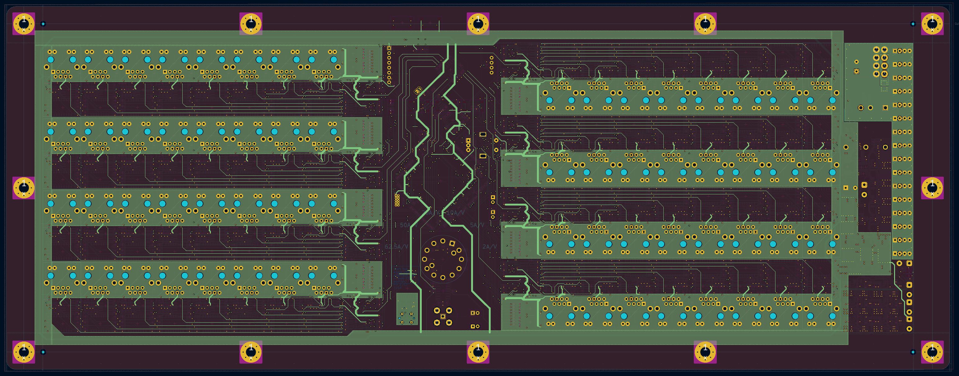
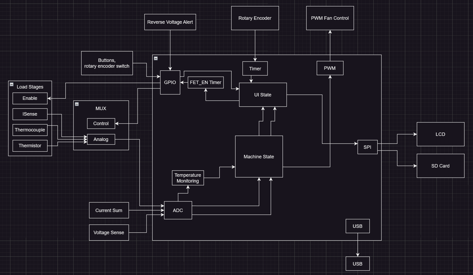
System Overview
The system consists of four primary parts:
- Load Stages - A single load resistor and it's associated switching and monitoring circuitry bundled in to one unit
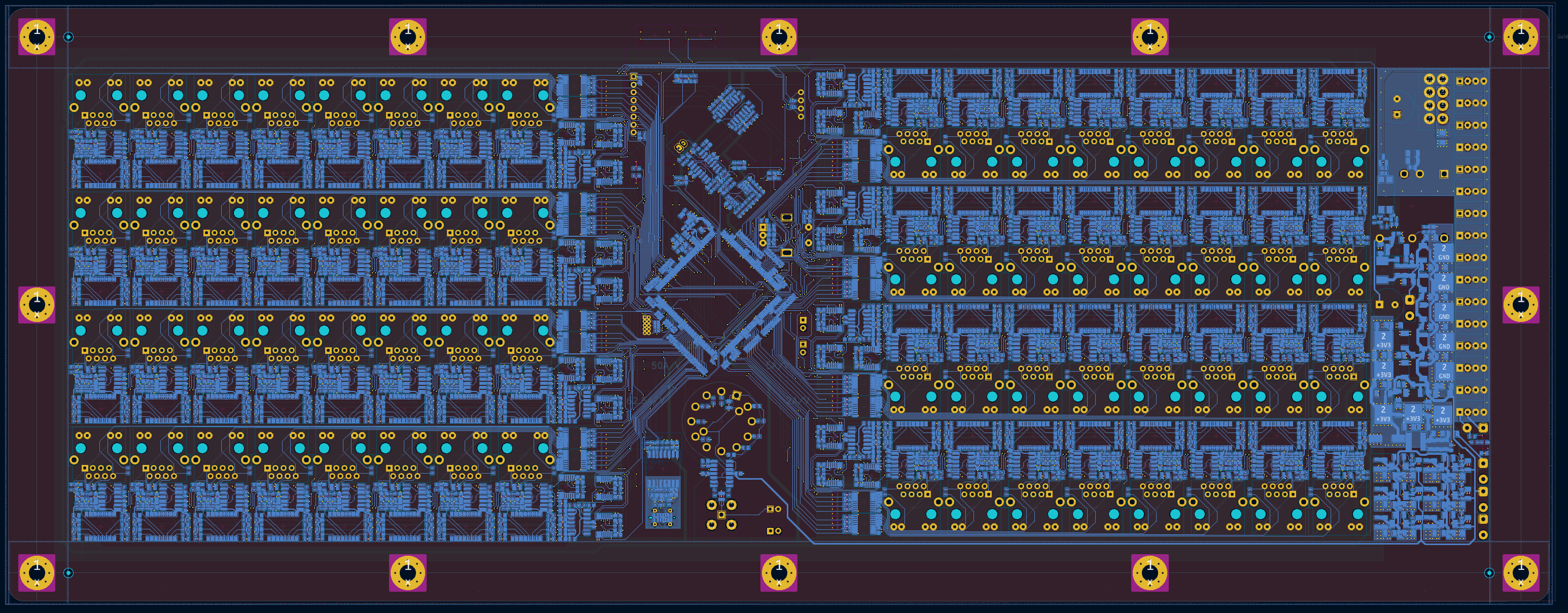
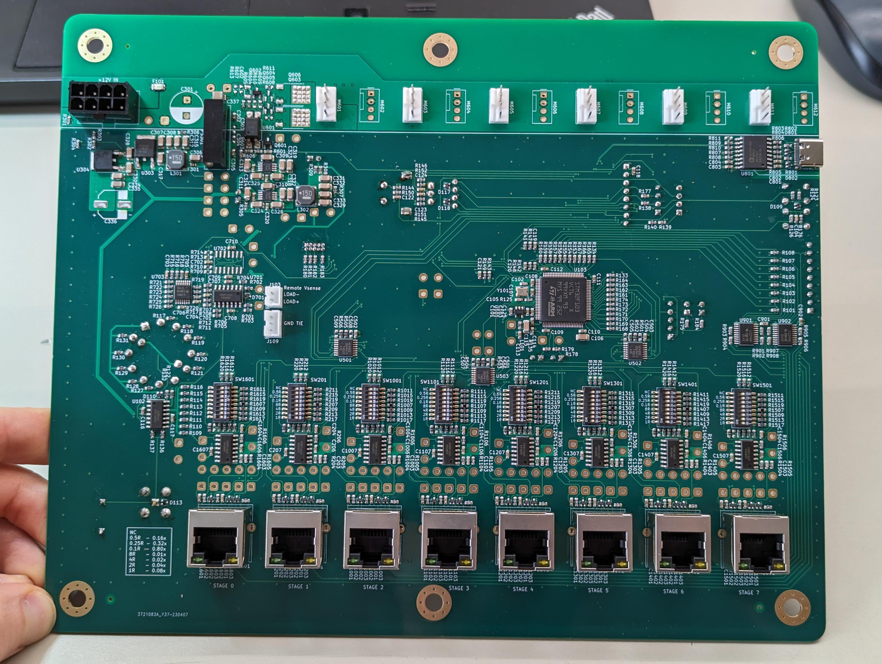
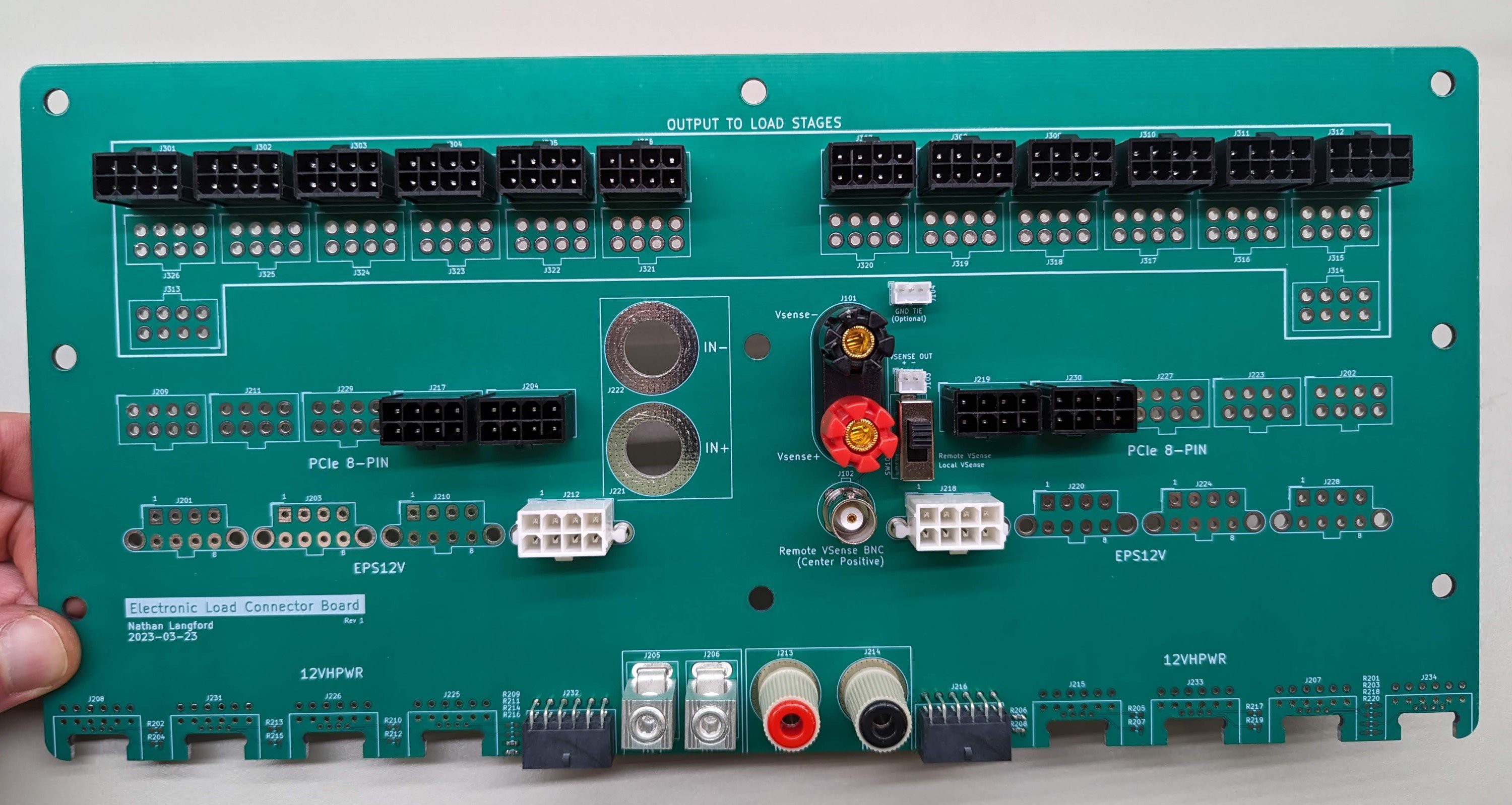
- Connector PCB - Any power supply being tested (which I'll call the DUT - Device Under Test) connects to the Connector PCB. From here cables are run to each load stage to distribute power.
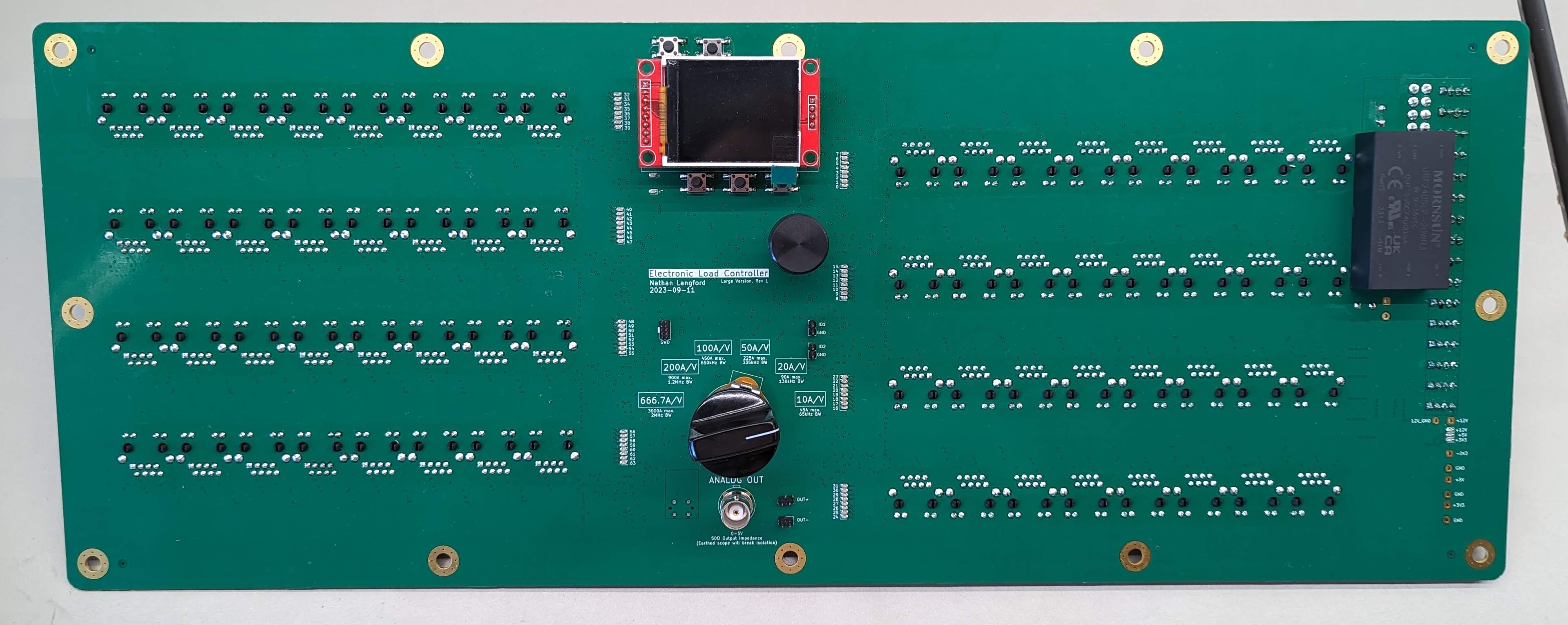
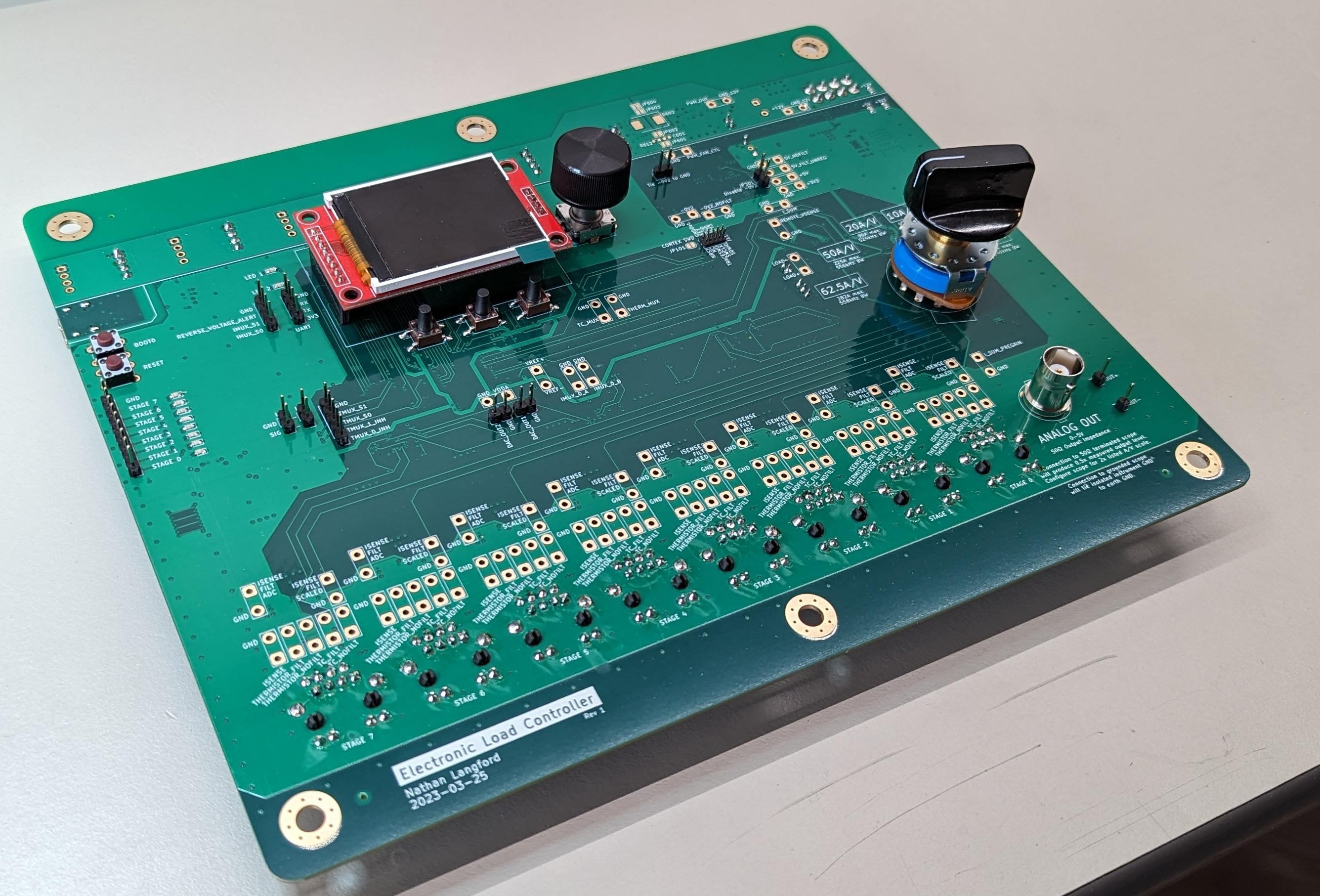
- Control PCB - The brains of the operation. Takes input from the user, and enables the correct combination of load stages to produce the desired load. Monitors temperatures and current of each load stage, produces an analog output current signal for an oscilloscope, and much more.
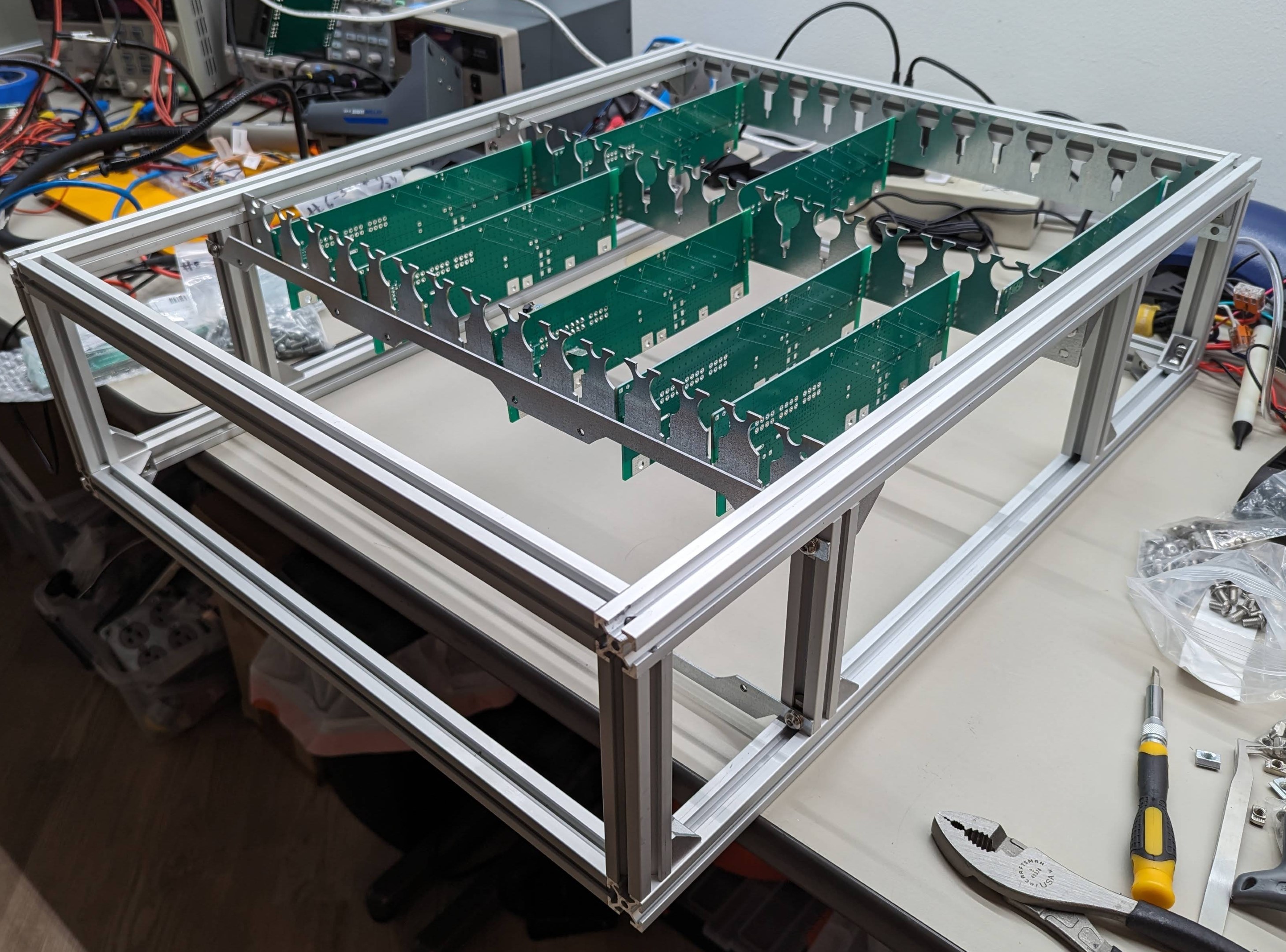
- Mechanical chassis - Holds all of the load stages and other boards, provides fan mounts for airflow, and is designed to be backed up to a window so all the heat can be dumped outside.
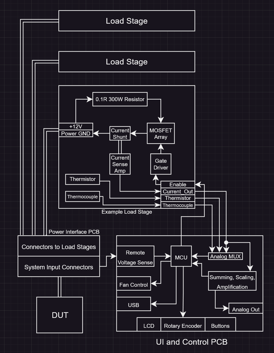
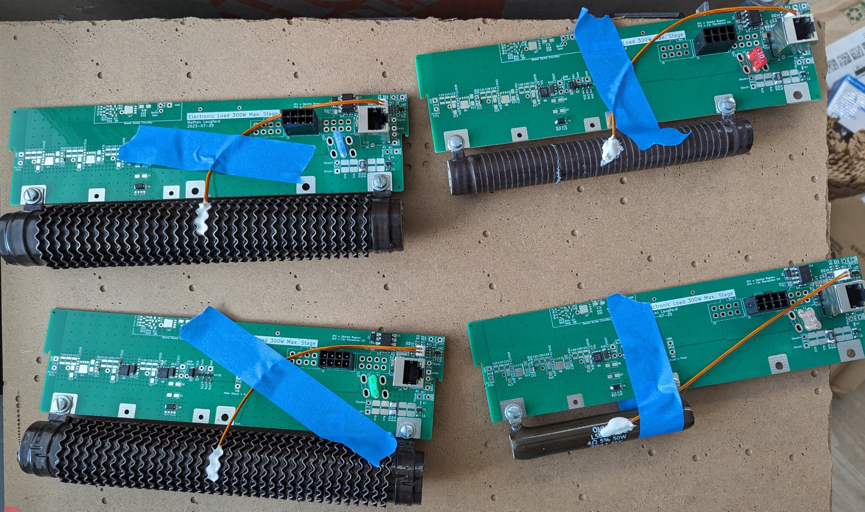
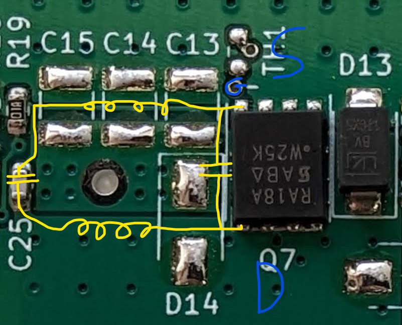
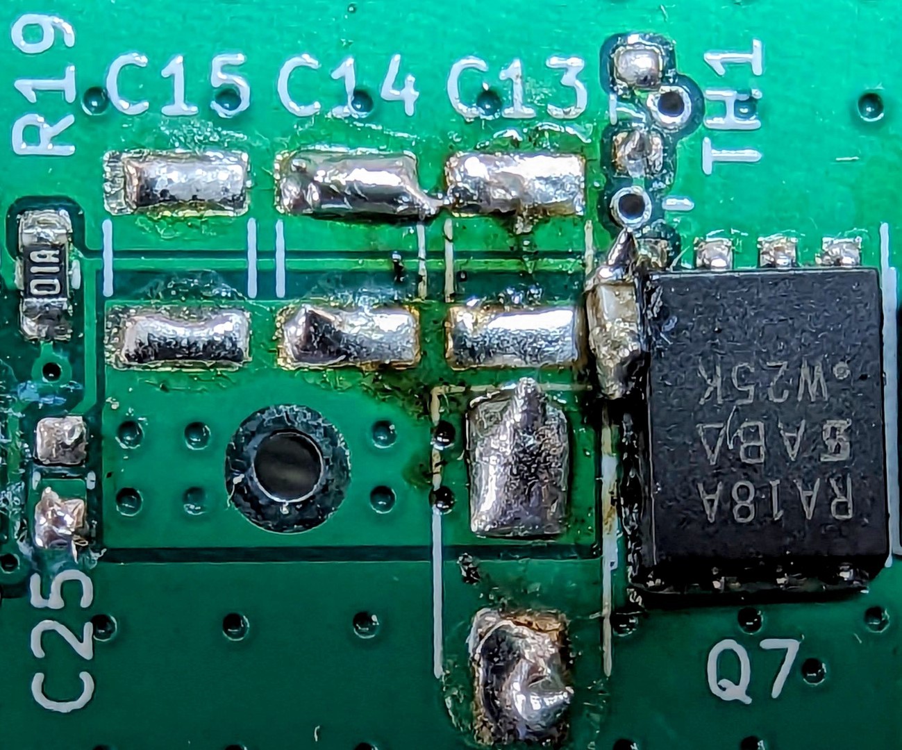
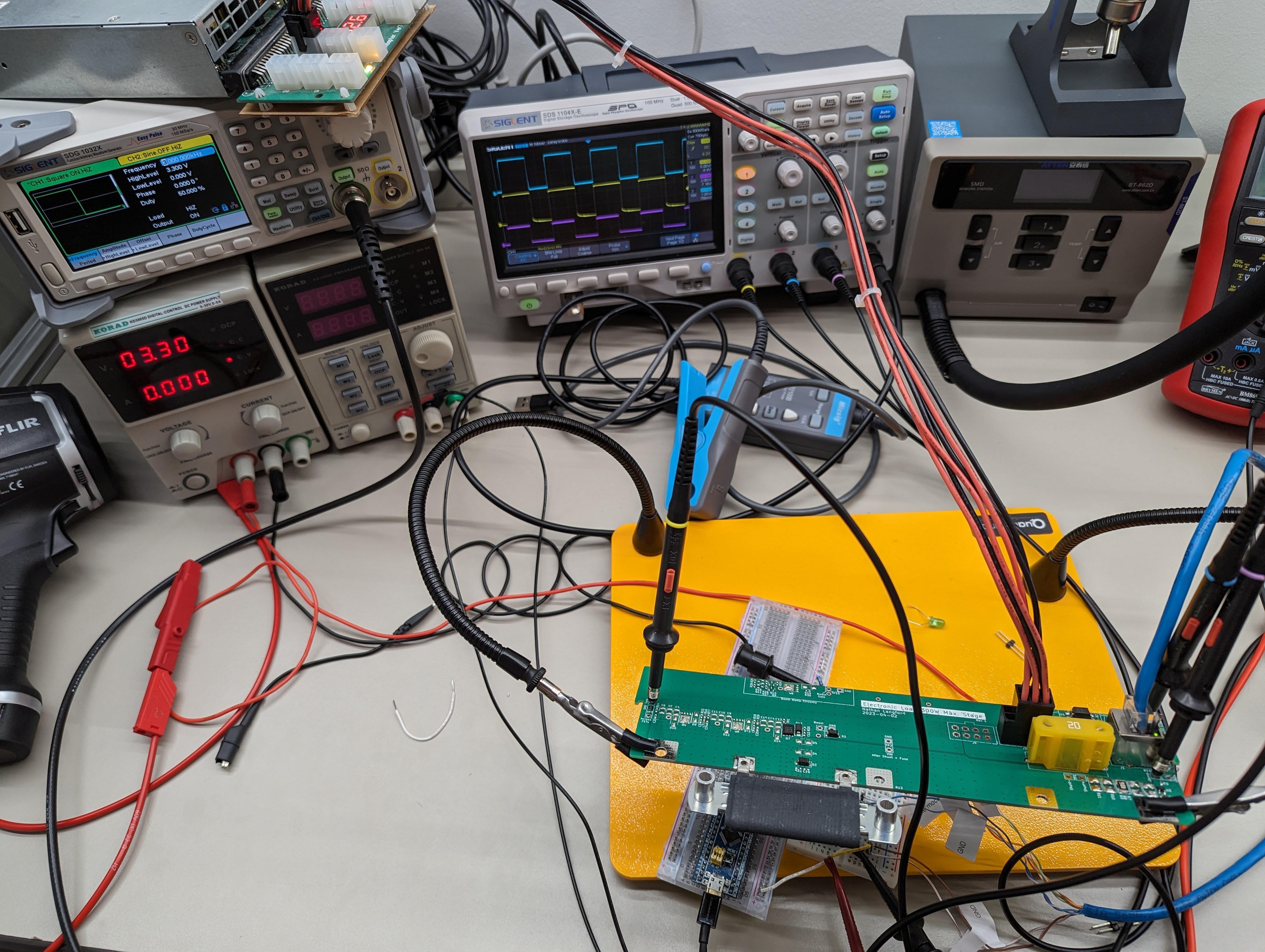
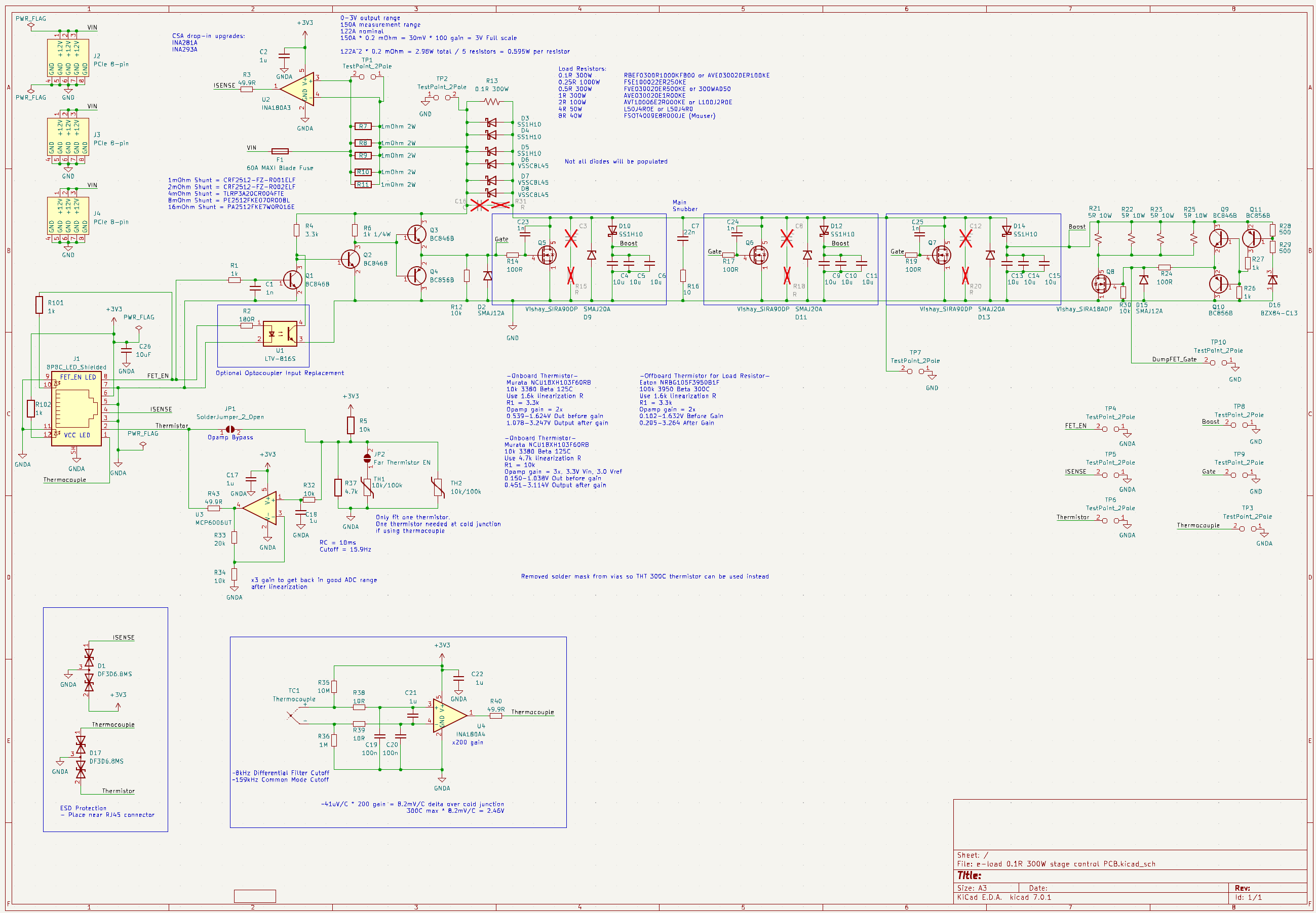
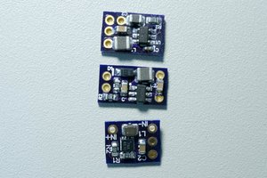
Load Stages
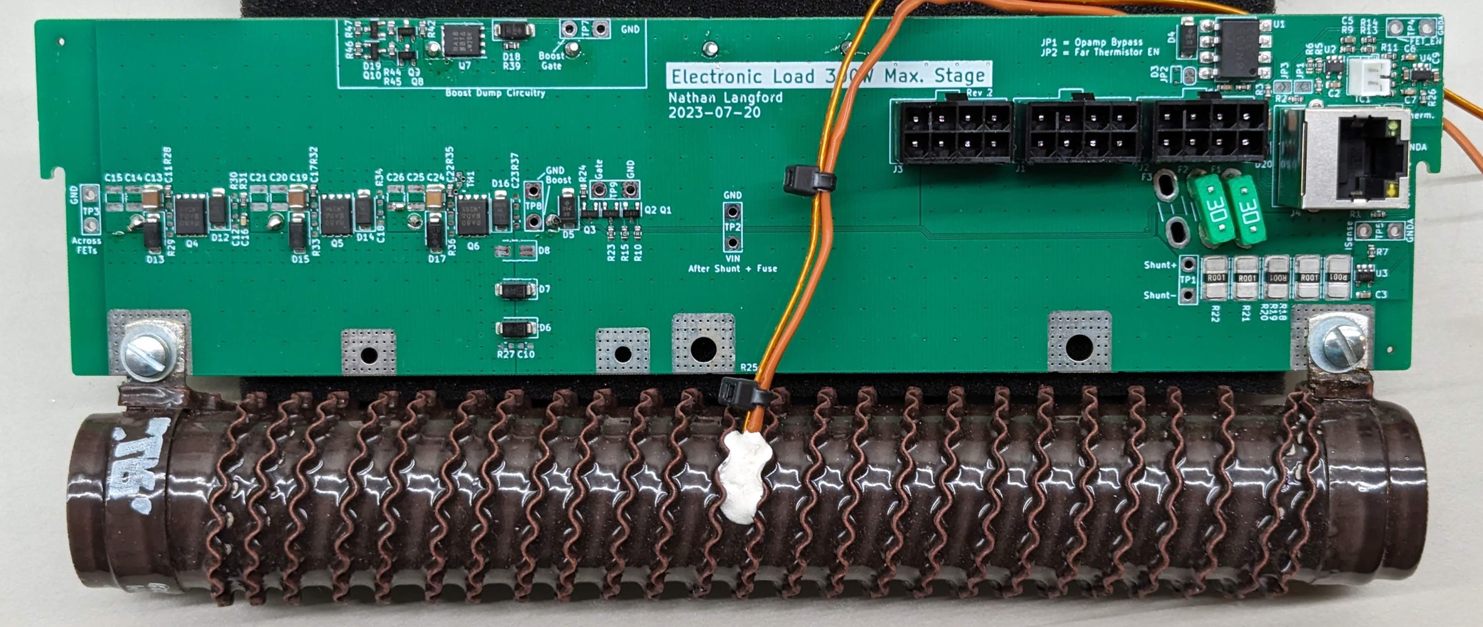
Each resistor will be attached to its own PCB to create what I'm calling a load stage. The load stages will all be connected in parallel to the system inputs. The load stages are self-contained and provide the following functions:
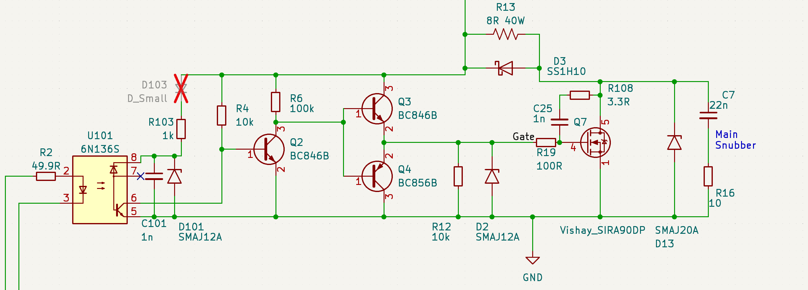
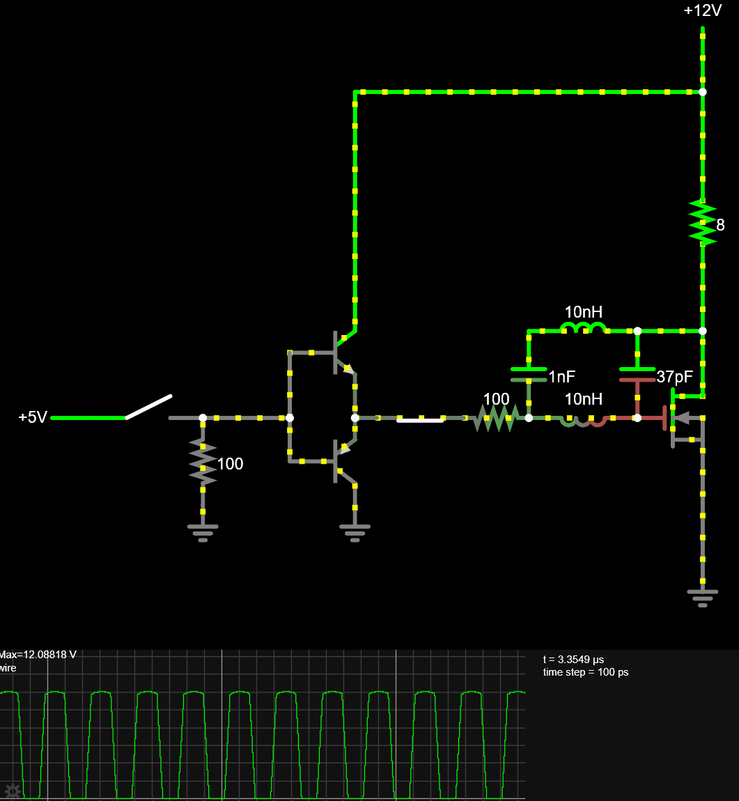
- MOSFETs to enable the load stage to consume power.
- Logic level input gate driver
- Isolated to prevent ground loops
- Using discrete components for lower cost
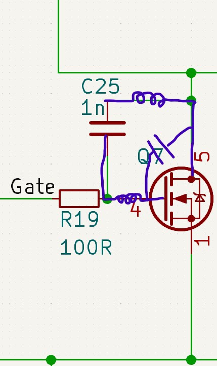
- "Boost dump" circuitry to capture the energy from the inductive spike on turn-off, and dissipate it slowly.
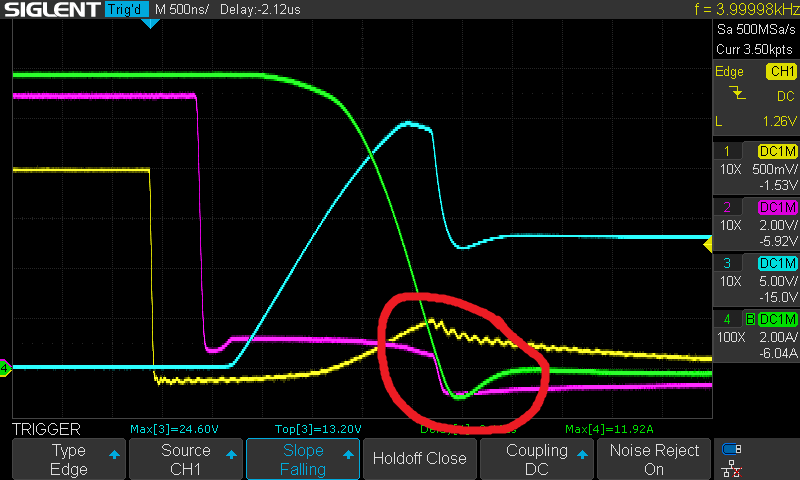
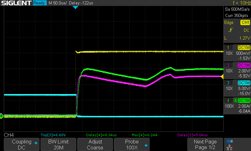
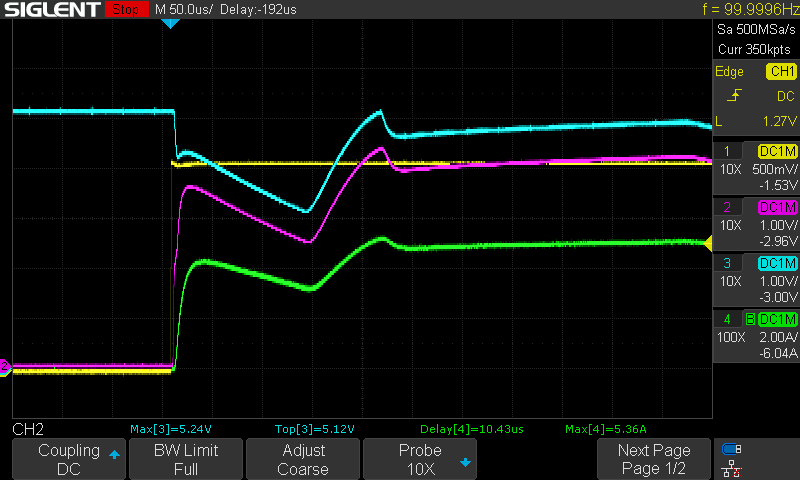
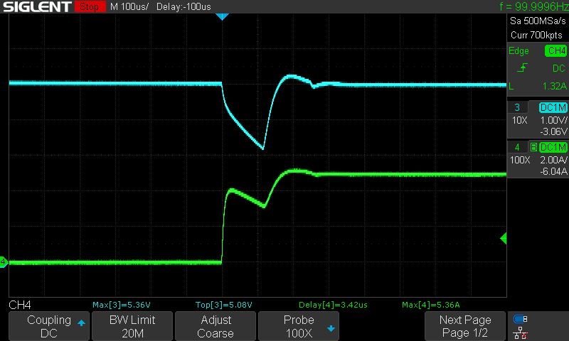
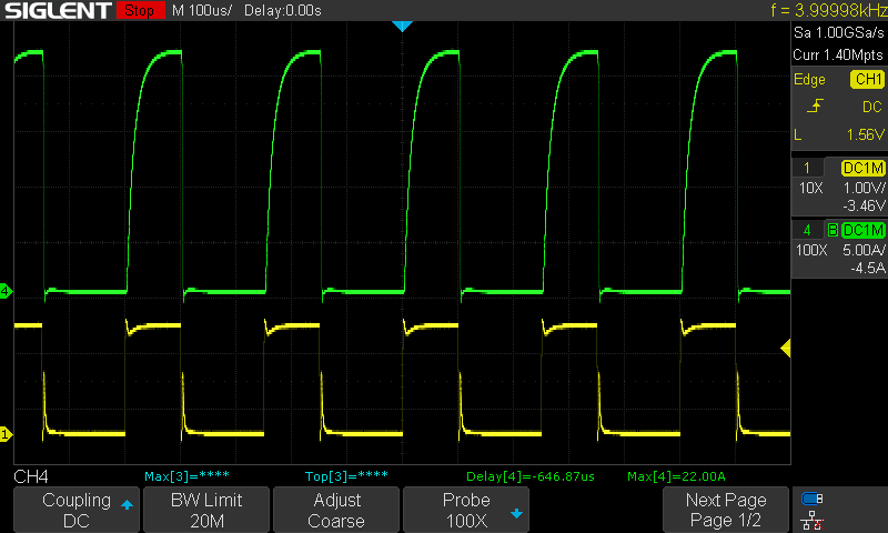
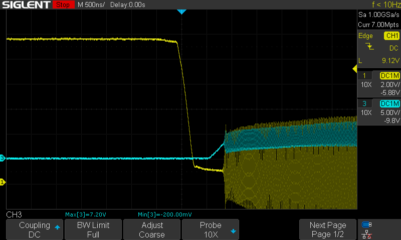
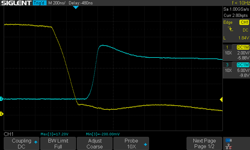
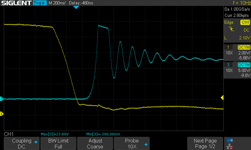
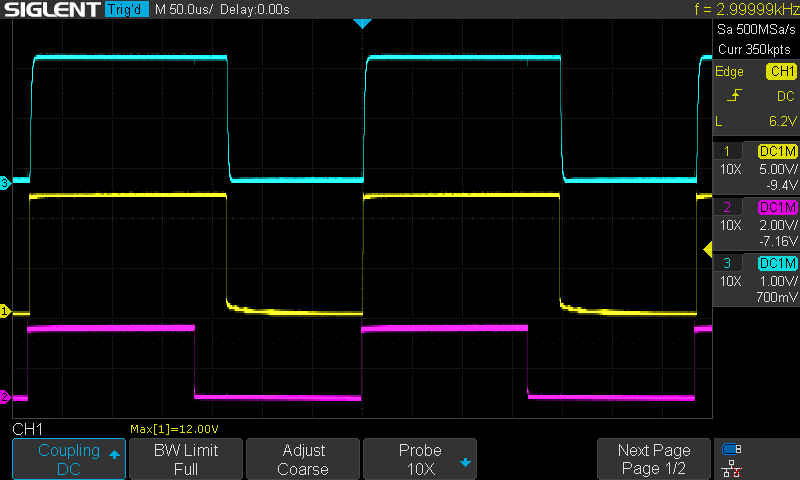
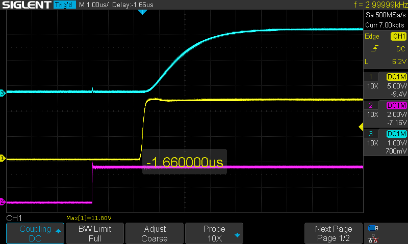
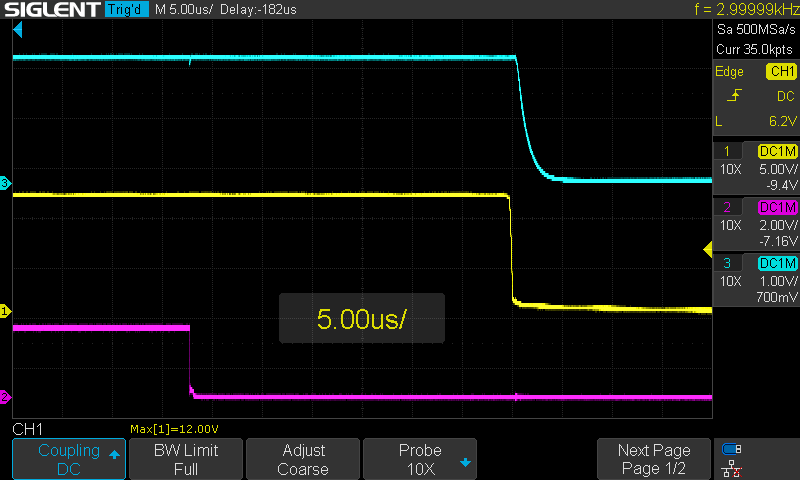
- When switching 122A repeatedly, the amount of energy stored in the inductance of the cables inside the system is large. Estimating 300nH total from the DUT in to the system, and then in to the load stage, that is 2.23mJ on each turn-off, or 7.37W at 3.3kHz. It gets even worse when you consider the inductance of the load resistor could be around 5uH. In simulation, this boost dump circuitry has to dissipate up to 30W when switching under a worst case scenario.
- Current measurement
- Thermocouple input and amplifier
- For measuring temperature of the load resistor to prevent overheating, and potentially compensate for their temperature coefficient of resistance.
- I'm actually using a INA180 current sense amplifier as the thermocouple amplifier. What cheaper way to get a 200x gain difference amplifier with very low input offset voltage?
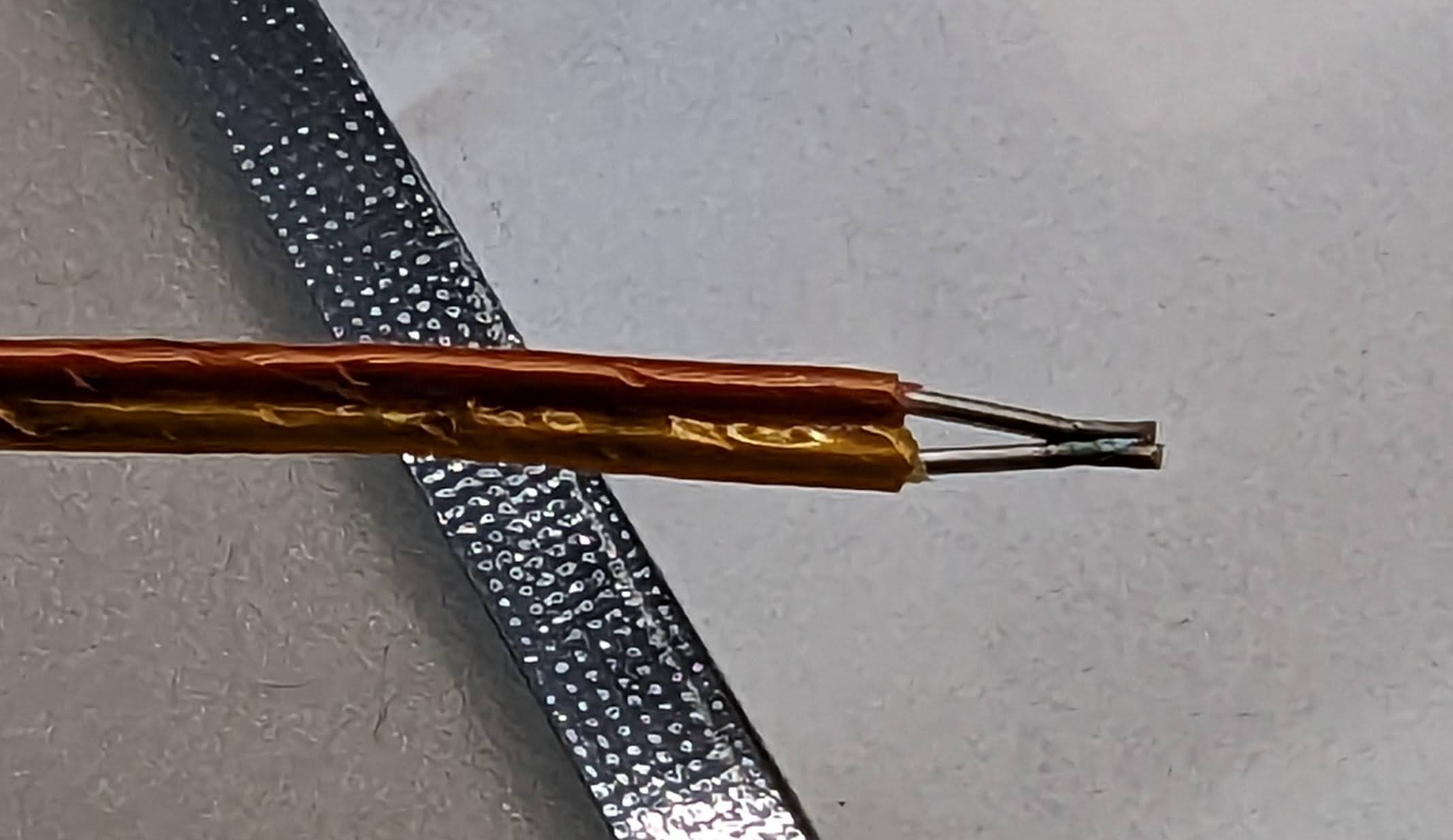
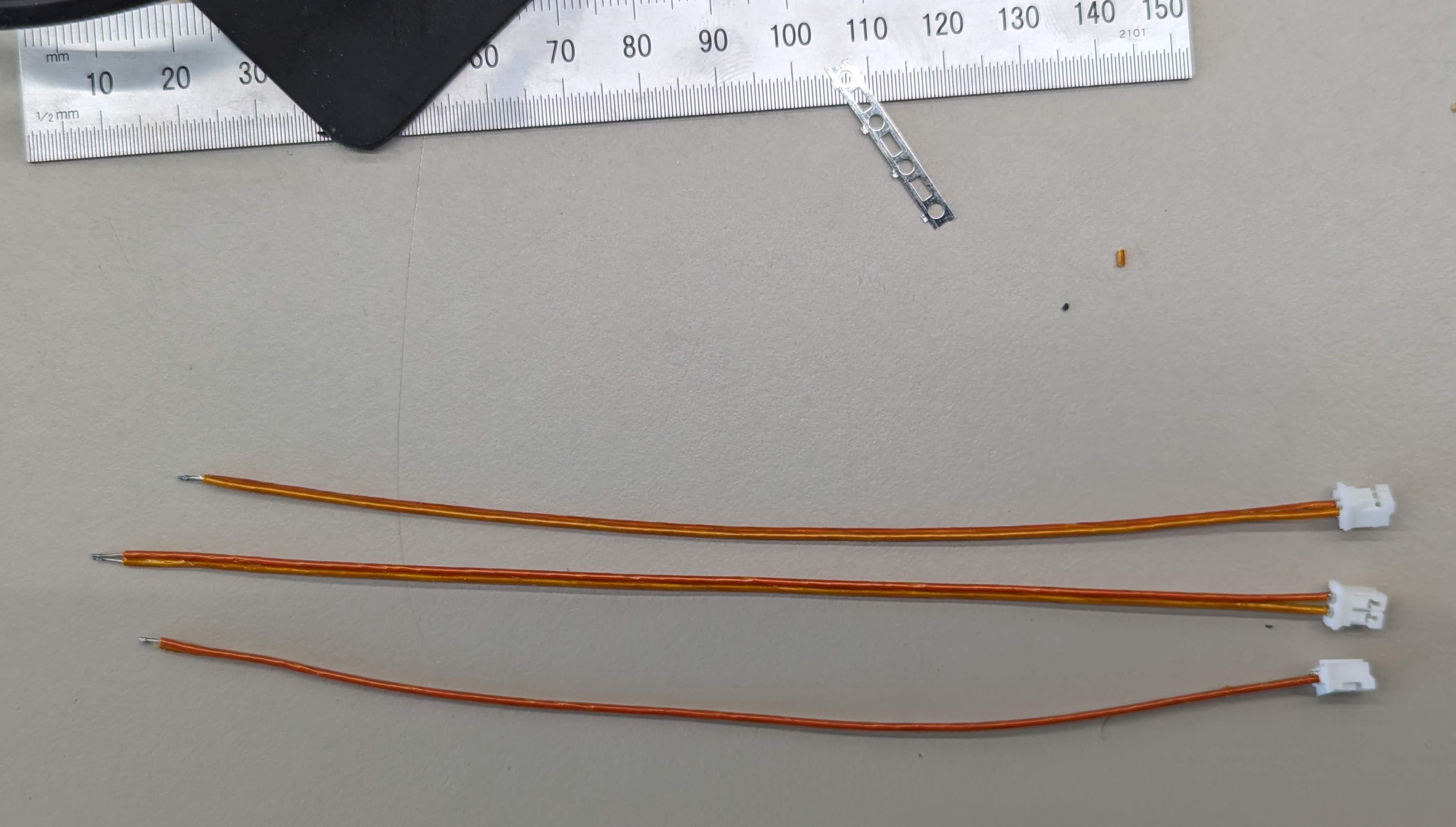
- I'm also making the thermocouples myself by spot welding thermocouple wire with a cheap Li-Ion battery-based spot welder intended for battery pack nickel strip welding.
- Thermistor for software cold junction compensation of thermocouple
Since each load stage is completely independent, the system can be easily scaled down to 1 load stage (although you only get one bit of resolution of load this way: off and on), all the way up to the 64 load stages needed to...
Read more »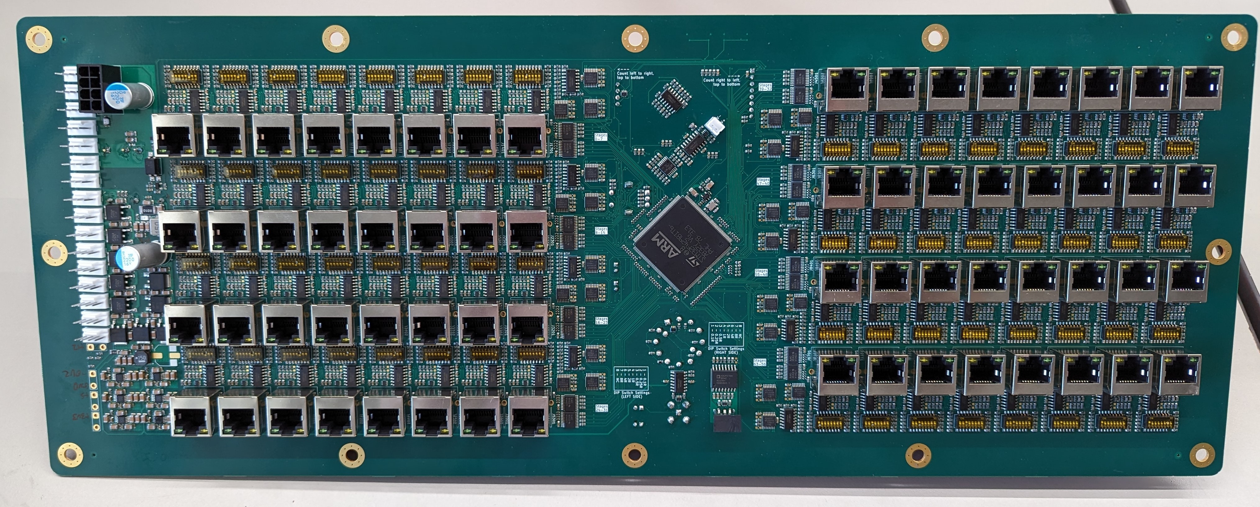


 Bud Bennett
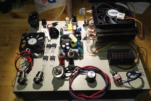
 Tron9000
 Bharbour
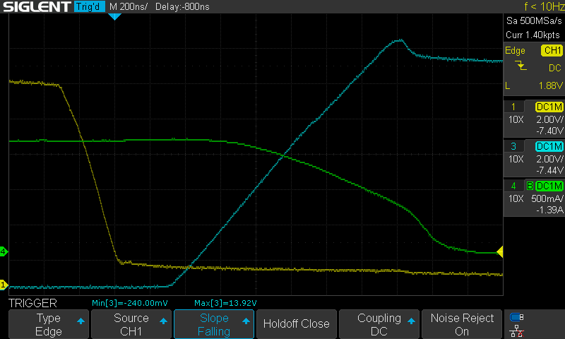
Hi, you might like to consider adding some control of di/dt, or how fast this load switches on and off to whatever current is selected. Big power supplies tend to be slow. Your early traces show the supply you use initially sourcing from output capacitance, that running out of charge, and then the supply control loop slowly catching up.
For testing a supply, you probably want to see how the supply works when the load switches on and off more slowly than the supply voltage control loop. Then later investigate what happens when the load switches quickly.