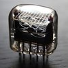
 Nixie
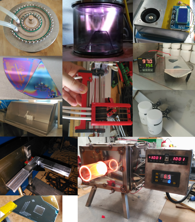
NixieTo build semiconductors at home, you need a 1000ºC oven with controlled atmosphere, a way to diposit metal on top of silicon and a safe way to handle deadly acids. There are also complementary tools, like a spin coater or a hot plate, needed to apply acid resistant film on top of the silicon, to etch away the patterns.
All that can be made at home with some ingenuity.
Two pdf "Books" have been created from all the research done for this project. (stored in the "Files" section.
- Semiconductors @ Home - Compendium! (all knowledge on the tools required for each process, the main focus of this project)
- Semiconductors @ Home - Cookbook! (a step by step guide to use the tools fabricated, under constant update)
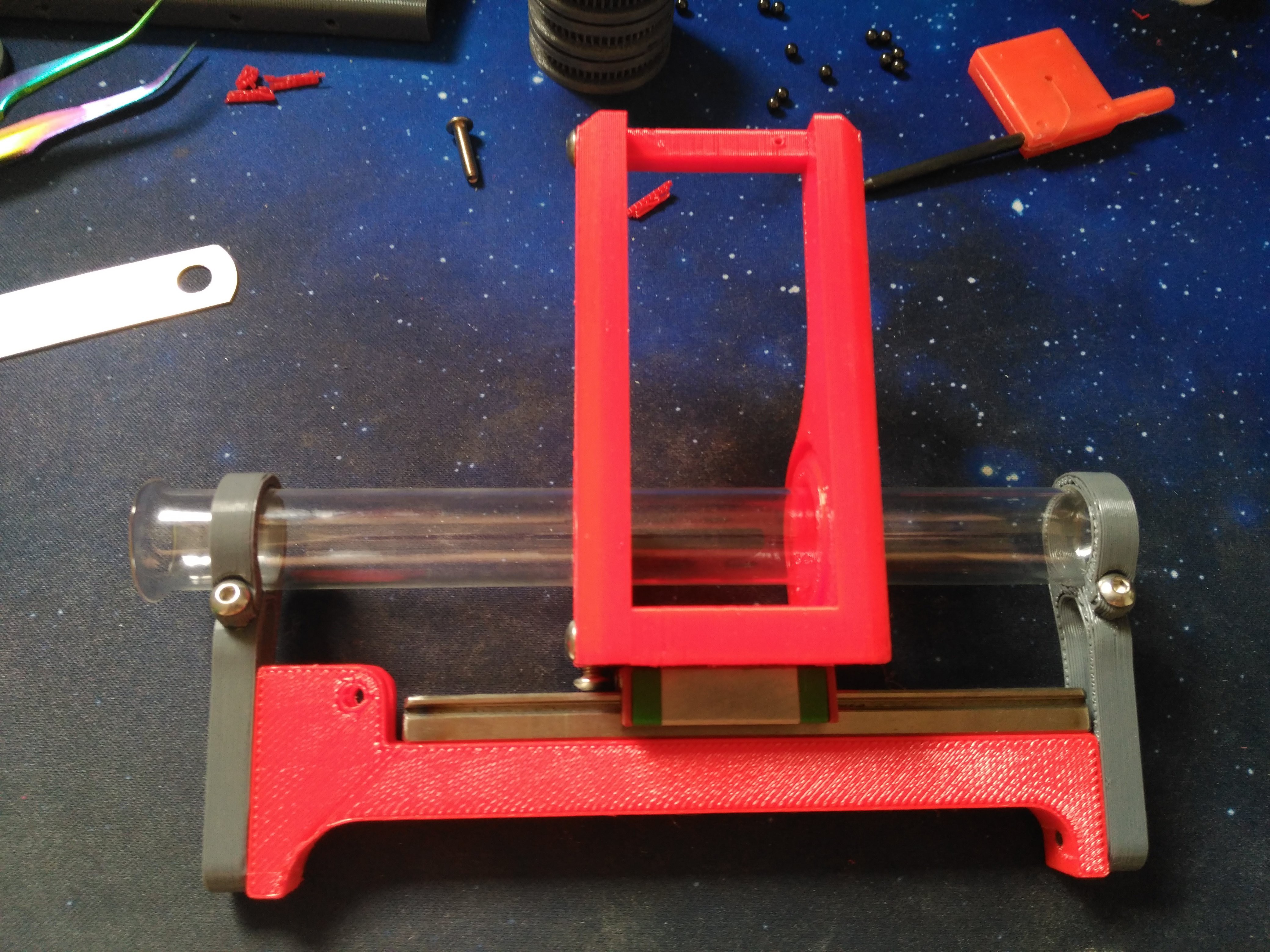
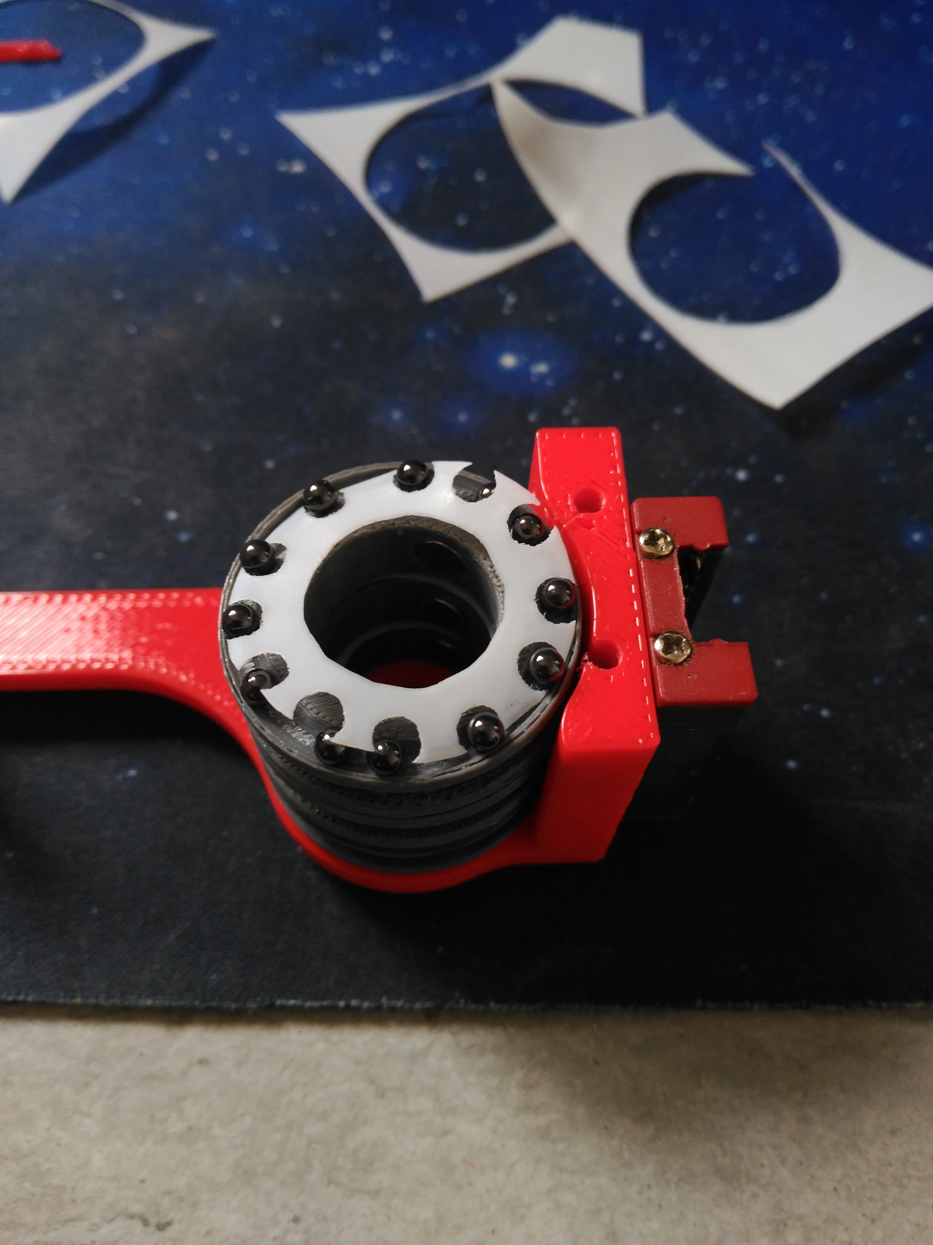
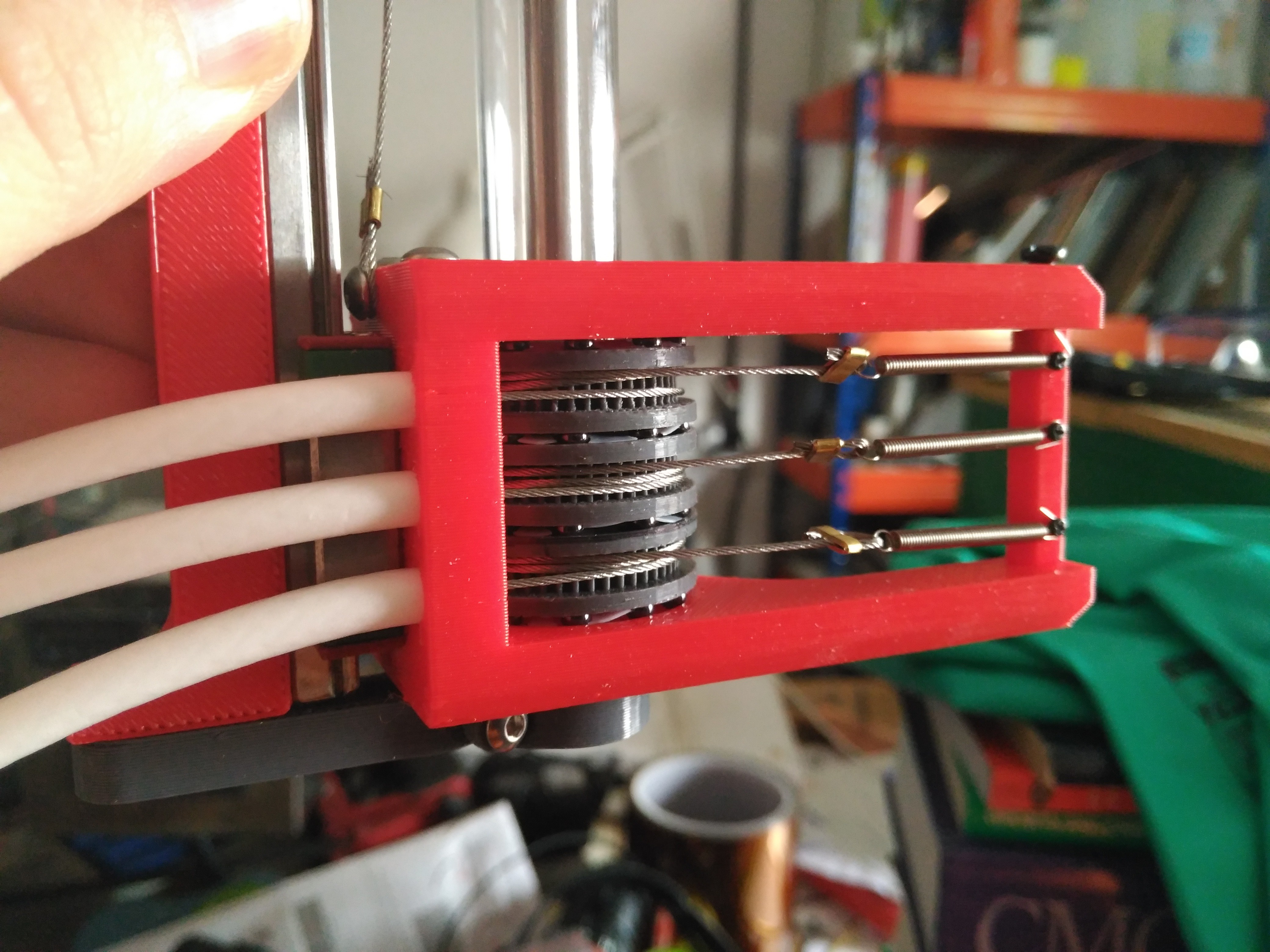
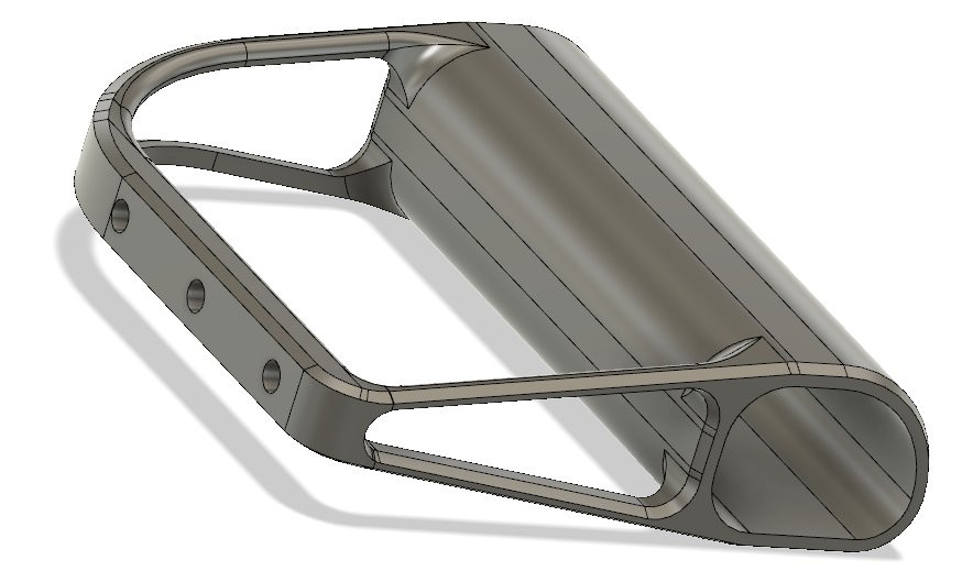
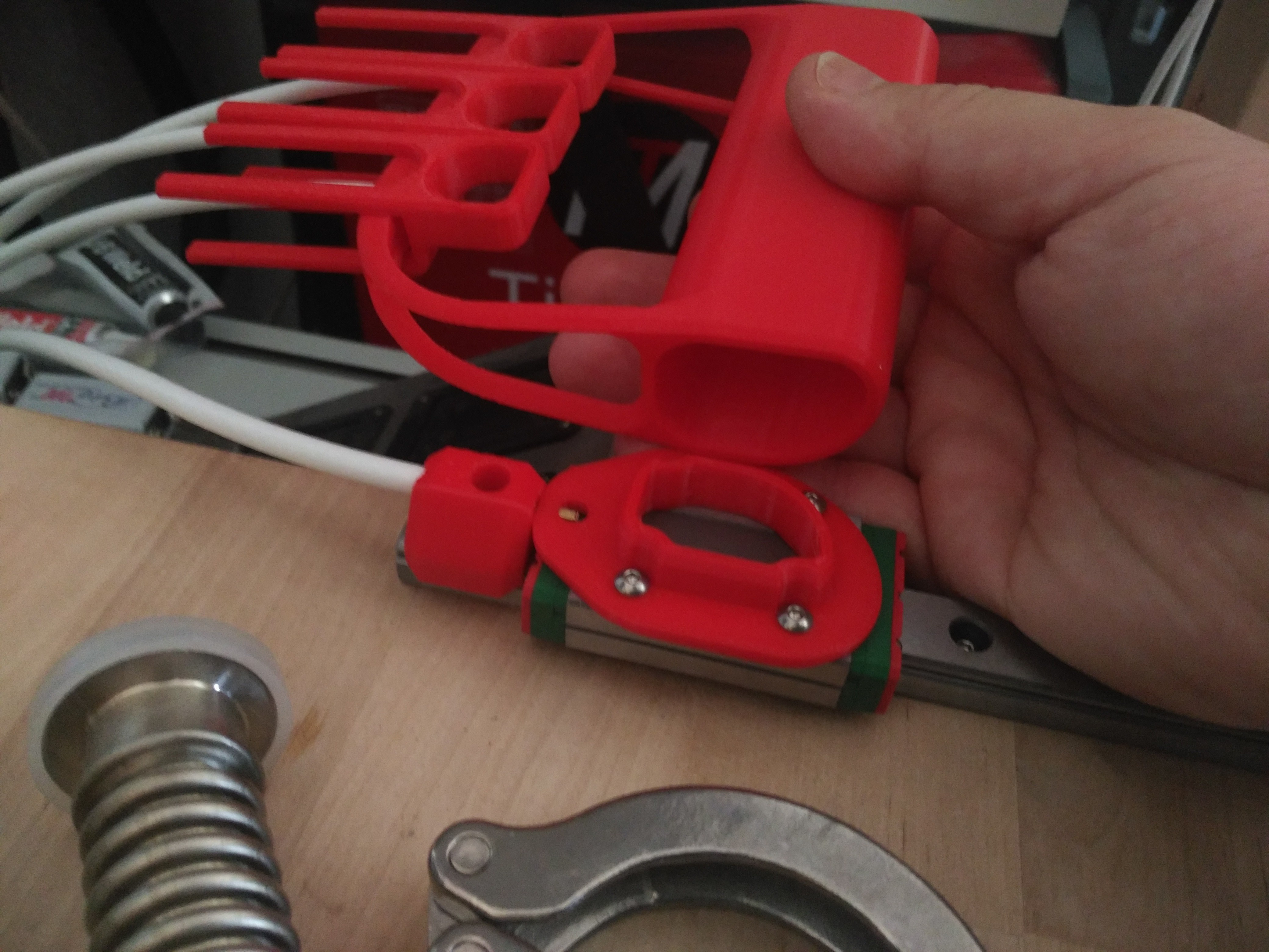
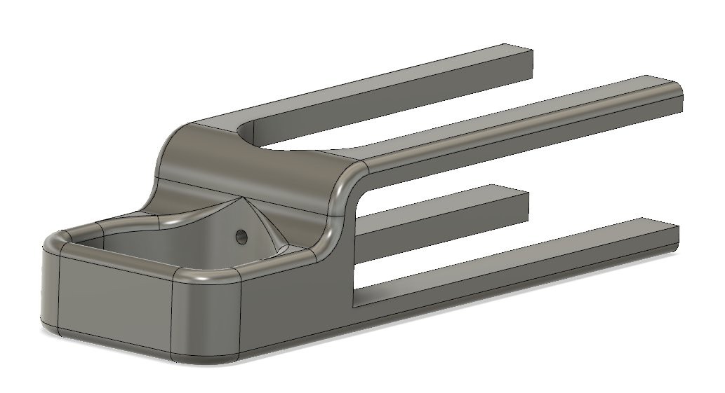
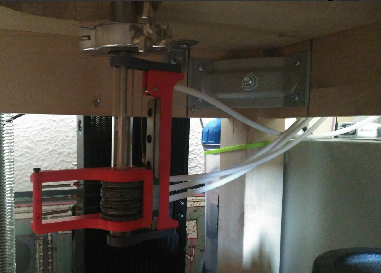
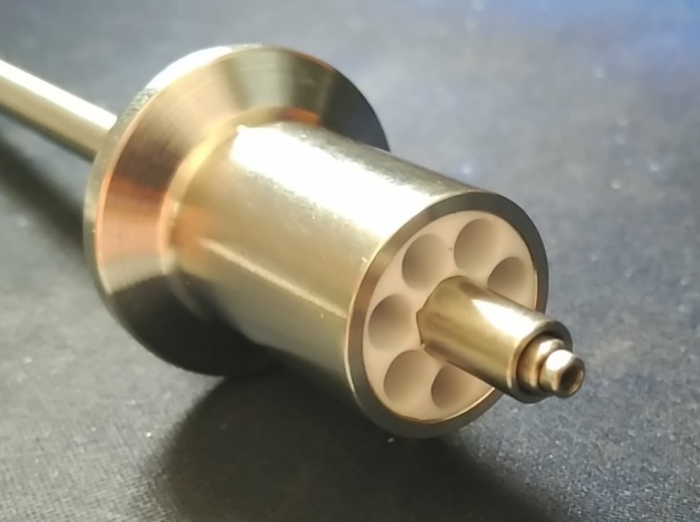
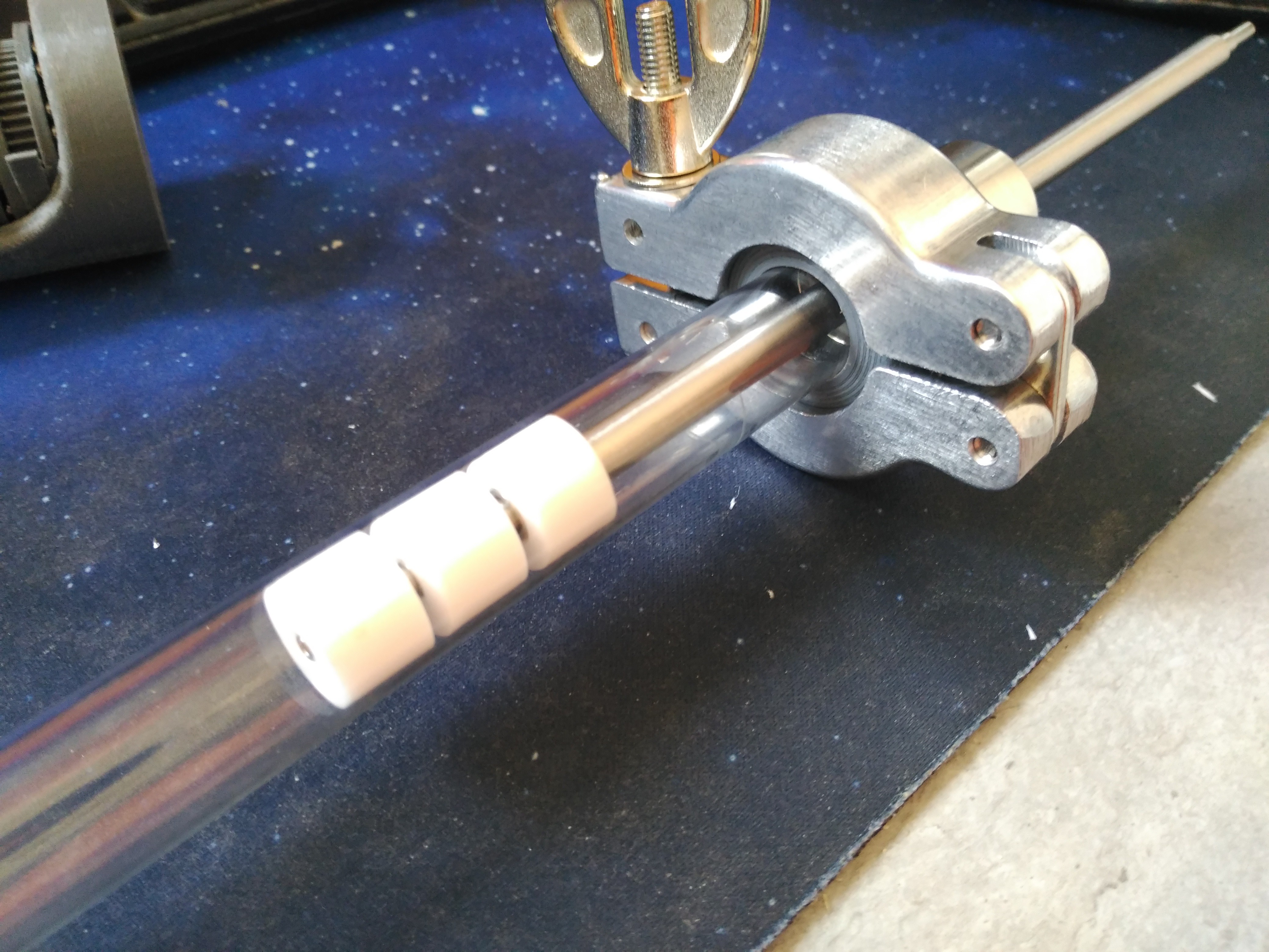
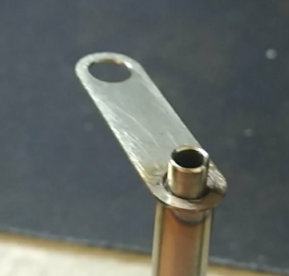
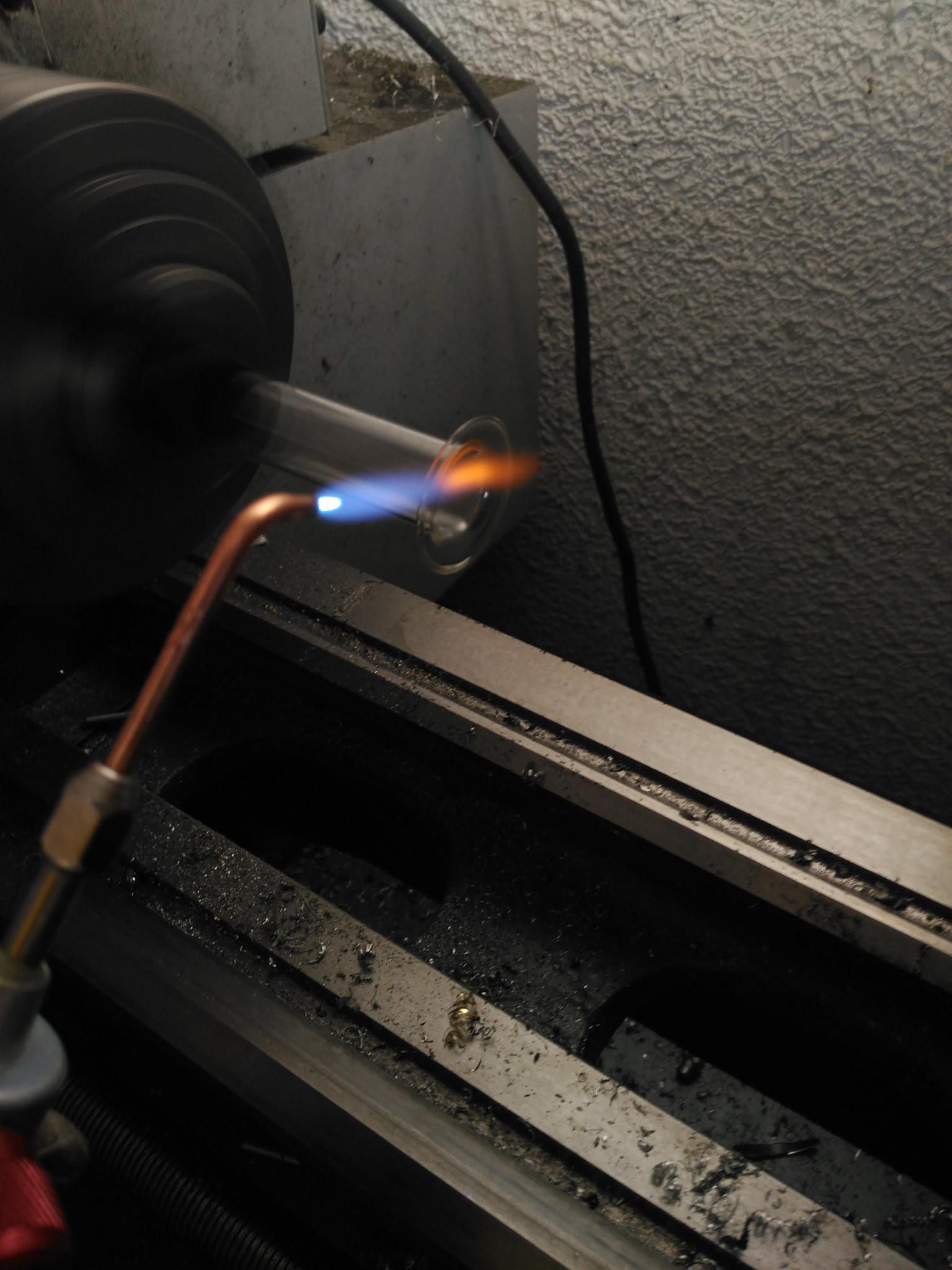
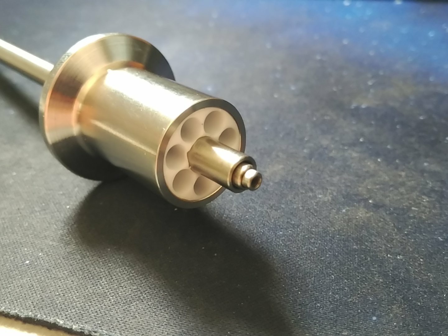
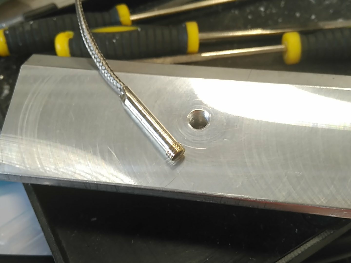
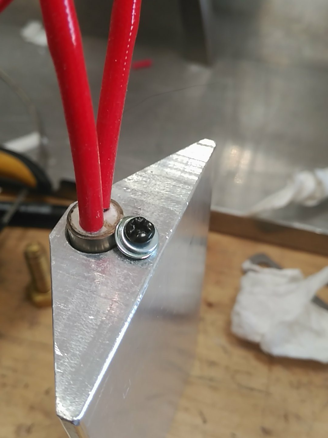
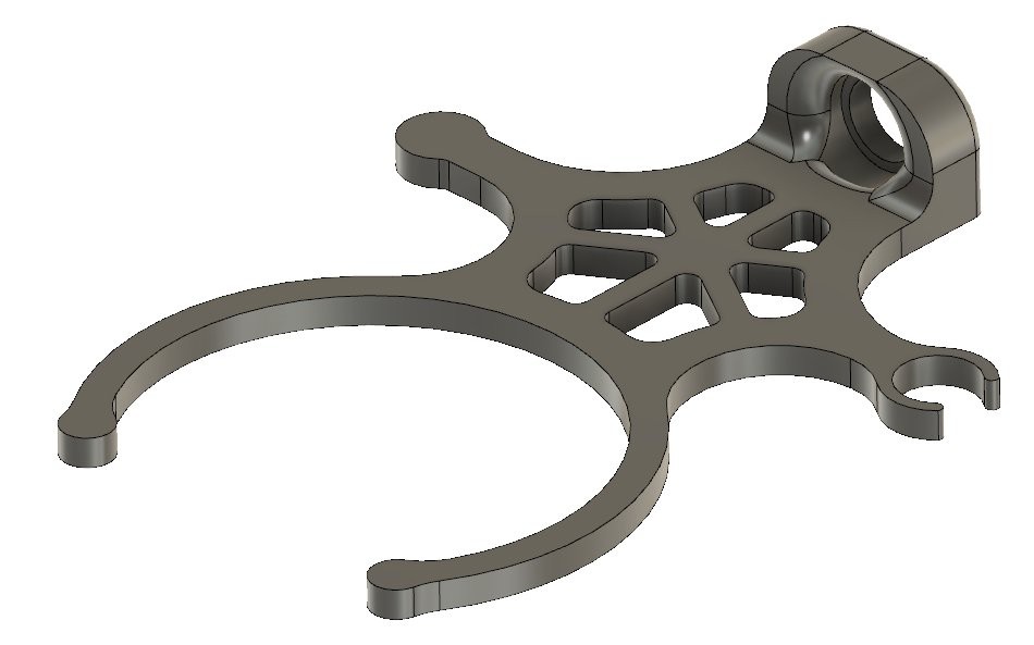
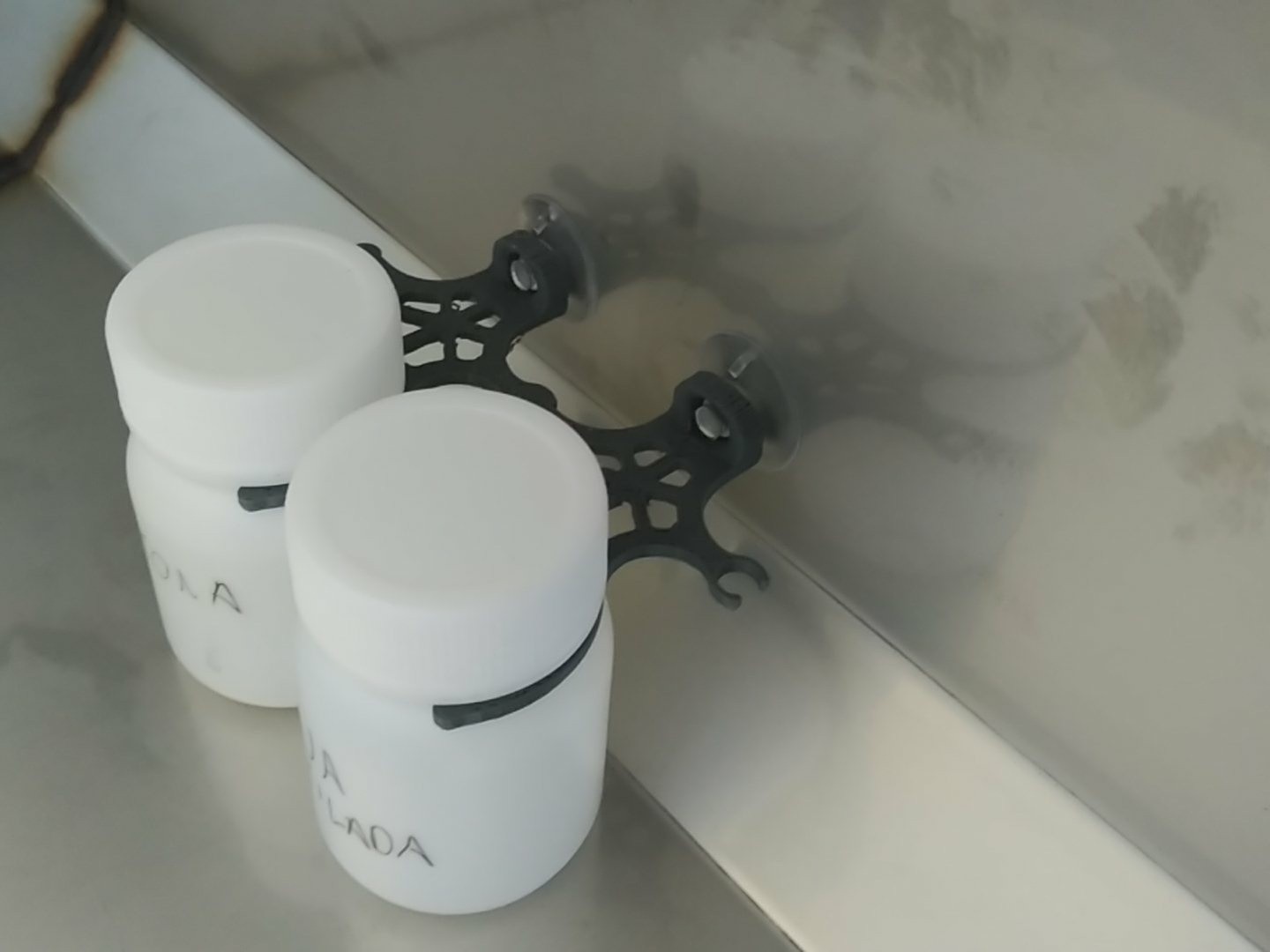
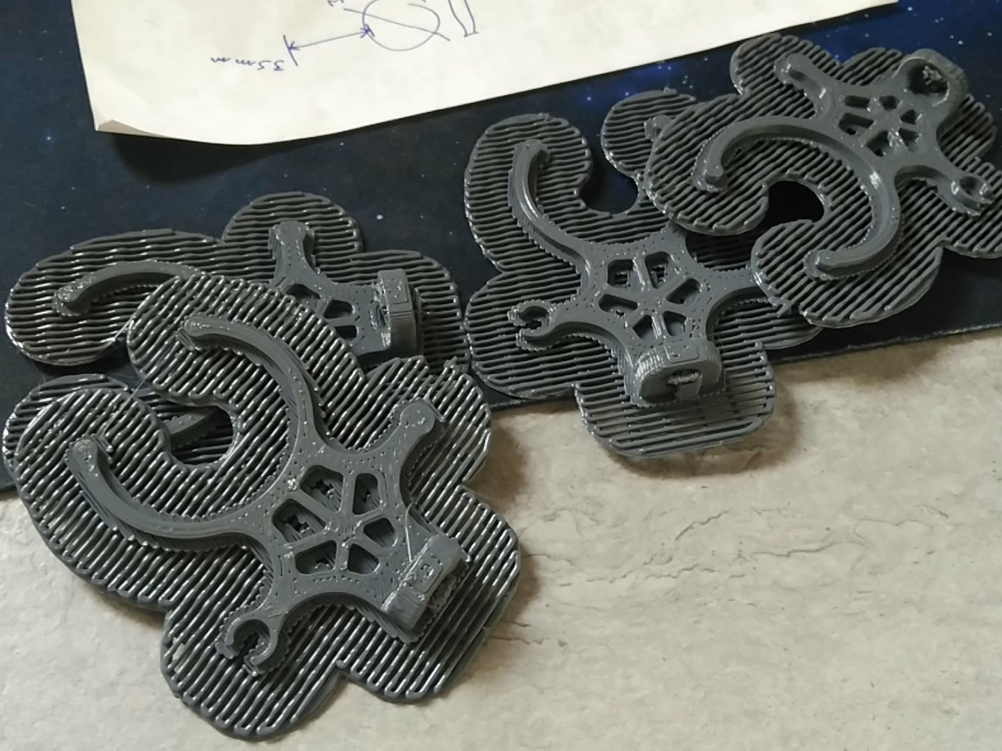
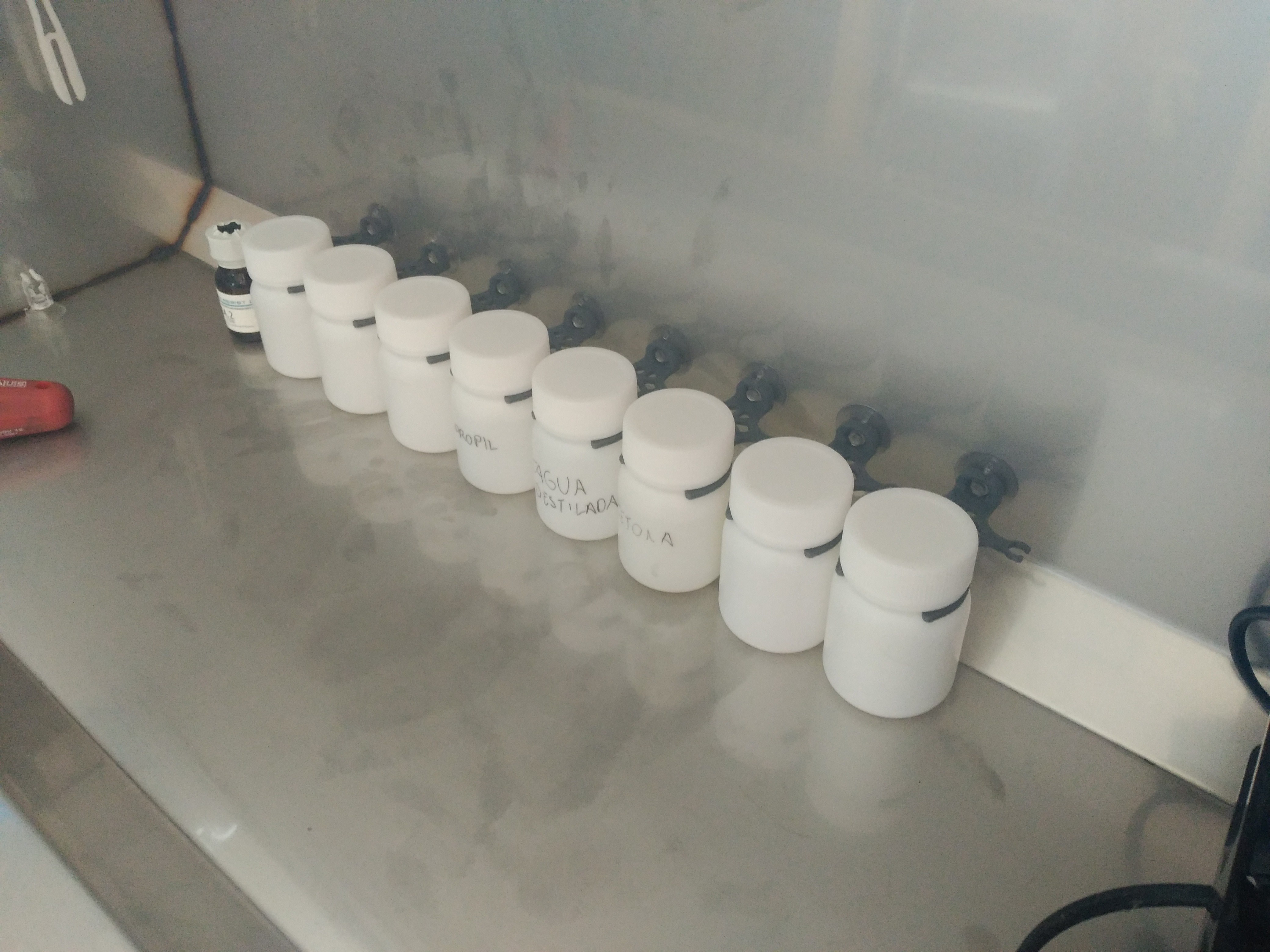
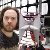
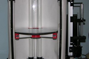
Below, some image highlights of the different tools and processes:
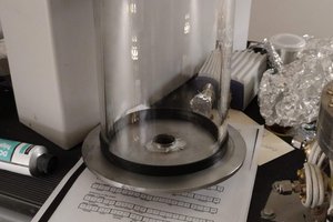
First diode, using Boron acid dopant in N-type silicon (phosporous):
For smaller resolutions, the plan is to investigate UV-curing resins and DiY e-beam maskless litography on PMMA, repurposing a CRT tube with a custom controller (already in prototype stage)
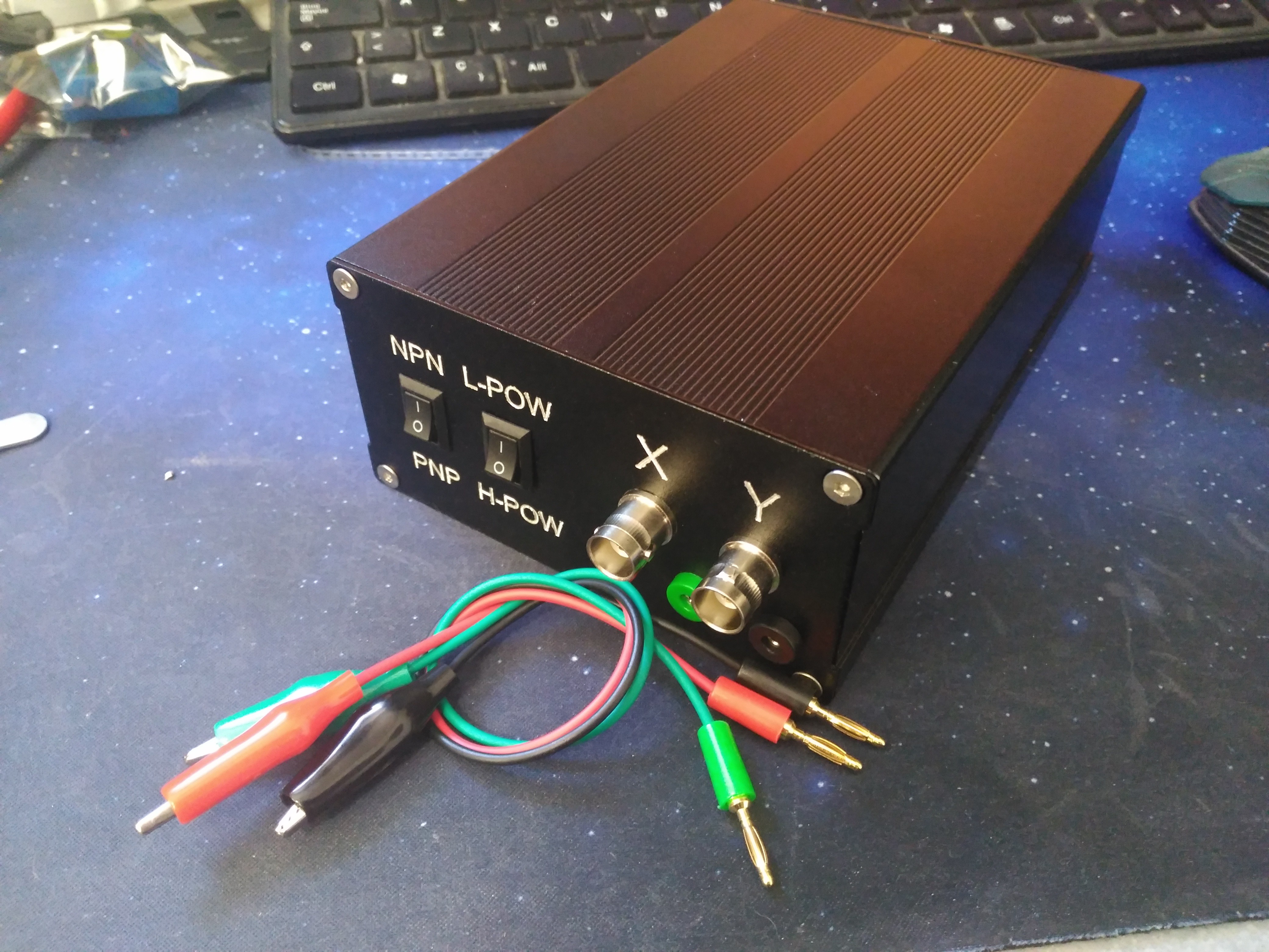
Once the semiconductor process is refined, vacuum wirebonding and DiY chip carriers will be tested.

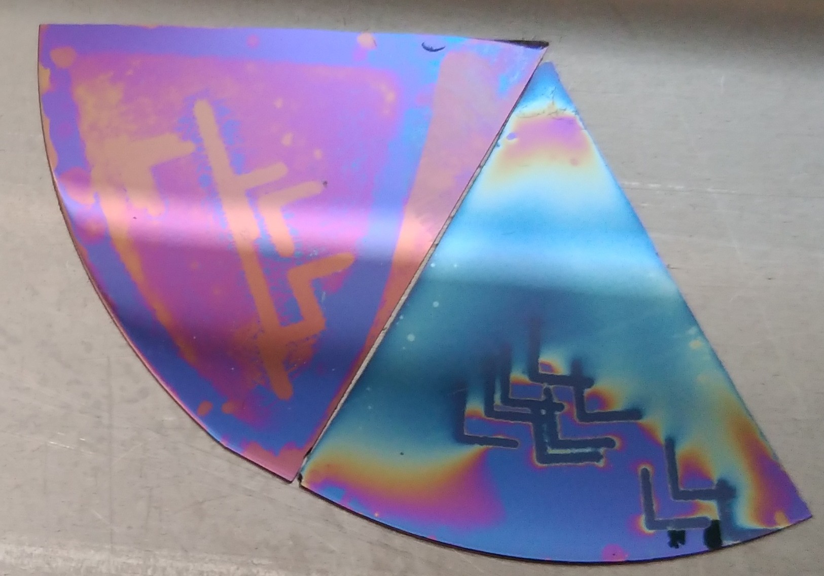
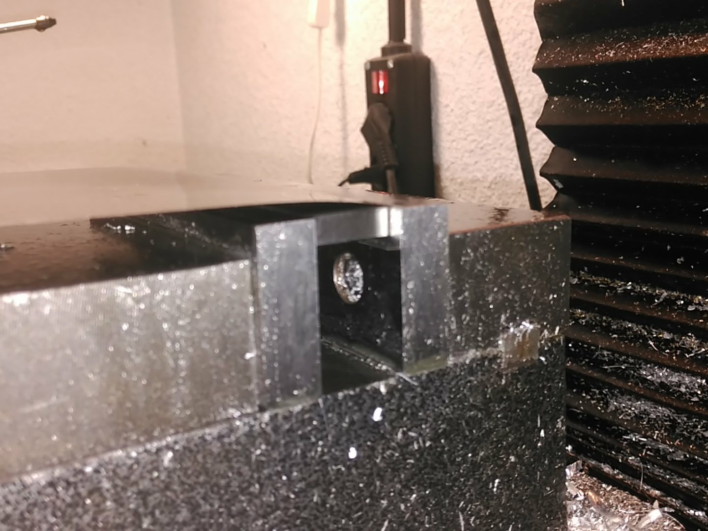
 (after diffusion, before etching)
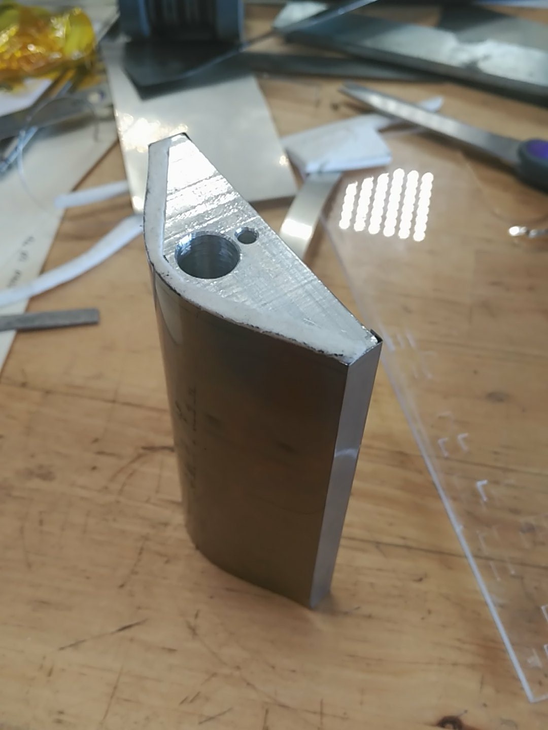
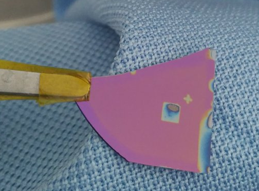 2mm test square and "+" fiducial. Should have left in HF longer, but curiosity got the best of me. ^^
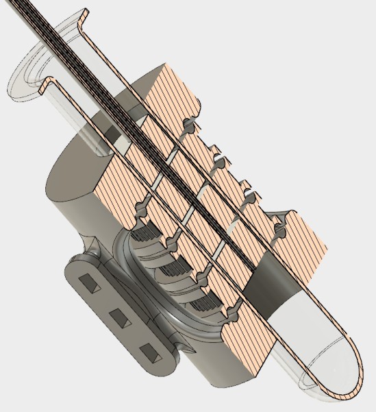


 Douglas Miller
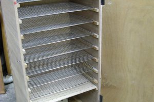
 shlonkin
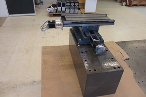
 rbalsan1
I just found this design for a DIY diffusion pump made from a cocktail shaker. https://diyvacuumtubes.com/steampunk-diffusion-pump-t14.html They have a few other designs on the forum as well. Only hand tools needed for this one.