-
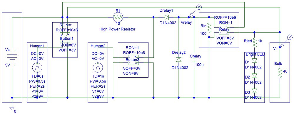
Two Button Relay Switch
12/29/2020 at 09:15 • 0 commentsThis article is based on information that was clearly explained in this link:
https://www.instructables.com/Two-Button-Relay-Switch/
I modified the circuit to replace the R2 resistor with a diode to improve the performance and reliability of the circuit in the link above.
Step 1: Design the Circuit
I used the PSpice student edition software version 9.1:
![]()
The light bulb can be replaced with a moderate current LED lighting source.
Step 2: Simulations
Transient (relay input voltage):
![]()
Transient (load voltage):
![]()
Conclusion
My circuit was not tested. However, I believe it can work.
-
Cooking Timer
03/28/2020 at 23:48 • 0 commentsThe circuit described in this article shows how you can use a capacitor and a transistor current mirror source to make a timer circuit.
Step 1: Design the Circuit
I have drawn this circuit in PSpice simulation software version 9.1:
![]()
The Db diode is used to protect transistors from buzzer discharging currents.
The buzzer and the LED turn ON when the Vbe2 (Q2 transistor base-emitter voltage) reaches the 0.7 V mark and the transistor turns ON, thus passing on the current to the next transistor cascaded stages:
Von = (Ve2 - Vbe2) = (2 V - 0.7 V) = 1.3 V
Where: Ve2 is Q2 transistor emitter voltage, Rv1 - Rv2 resistors connection node (2 V), and Vbe2 is Q2 transistor base-emitter voltage (0.7 V).
The switch is used for discharging the Ct1 and Ct2 capacitors to reset the timer.
Now we can do timing calculations:
Discharge time:
We all know that the total value of parallel capacitors is the sum of all connected parallel capacitors. Let's assumed that Ct1 and Ct2 are both equal to 500 uF to simplify our calculations because you can also use a 1000 uF capacitor instead of those two capacitors.
The capacitors are fully discharged after 5 time constants:
5*Tc = 5*Rdc*(Ct1 + Ct2) = 5 * 100 * 1000 uF = 0.5 seconds
Charging time:
i = C dv/dt
Thus:
dv = (1/C) * (i*dt)
and
dt = C*dv / i
Imax = (Vs - Vbe1) / Rt2 = 2.3 V / 10 kohms = 230 uA
Imin = (Vs - Vbe1) / (Rt1 + Rt2) = 2.3 V / 1010000 ohms = 2.27722 uA
Maximum time to turn ON:
TimeMax = (Ct1 + Ct2) * (Vs - (Ve2 - Vbe2)) / Imin = 1000 uF * 1.7 V / 2.27722 uA
= 1000 * 1.7 V / 2.27722 = 746.5243 seconds
You can double the charging time by increasing capacitor values or Rt1 variable resistor values. There are 2 Megohm variable resistors sold on the internet.
Minimum time to turn ON:
TimeMin = (Ct1 + Ct2) * (Vs - (Ve2 - Vbe2))/ Imax = 1000 uF * 1.7 V / 230 uA
= 1000 * 1.7 / 230 = 7.3913 seconds
Step 2: Simulations
Simulations show that our calculations match the results:
![]()
The green curve shows how the Q4 transistor pair saturates at about the 640-second mark. This is below the predicted 746.5243 seconds time to turn on because I used three cascaded transistor stages that amplify the Q2 transistor input signal. Thus the circuit is already ON a few seconds before the Vbe2 (Q2 transistor base-emitter voltage) reaches the 0.7 V mark.
-
Reducing Transistor Power Dissipation
03/06/2020 at 08:17 • 0 commentsIn electronic industry putting two transistors is a method that is often used to reduce the power dissipation across each transistor.
Watch this YouTube video:
After watching this video do not forget that you do not need a resistor for each transistor. They can share one base transistor and one collector or emitter transistor, depending on the transistor configuration.
However, putting transistors in parallel is not well spoken off. Here is the circuit that I have drawn in PSpice software. Do you think it is a good circuit?
![]()
You might have assumed that connecting two transistors placed in series will ensure that each transistor will only need half the maximum collector emitter voltage. However, this is not the case because one of the transistor could be saturated and the other will be dissipating almost the entire power supply voltage from its collector to its emitter if the collector current is low. Thus this circuit is also lacks linear characteristics that a parallel transistor circuit will have. This is why this is a bad circuit for reducing power dissipation.
However, the circuit above can be modified and become useful for other applications. Zener diodes can be placed in parallel with transistors and an LED with resistor can be placed in series with the collector. This will allow four channel control of four LEDs with a 9 V battery. Suppose each transistor has a maximum collector emitter voltage of 5 V (this is just an example because a typical BJT transistor would have maximum collector emitter voltage of 30 V and a typical LED does not need much current/power at all), the Zener diodes will ensure that this voltage is not exceeded even if the power supply voltage is doubled. However, even Zener diodes have maximum voltage, current and power ratings. You can connect four transistors in parallel with a 680 resistor in series with the LED. However, this will lead to power loss, due to power dissipated in the resistor. This is why this modified circuit is could be a better solution the four channel LED controllers or motor/relay drivers.
![]()


 Benjamin Prescher
 MrWunderbar
 will.stevens
 Alain Mauer
 Boxerbomb
 Thomas Snow
 Laetitia BEL
 Benjamin Blundell
 NaranInc
 Saad_u_rehman
 Amirreza Nasiri
 Andrea De Napoli
 Peter McCloud
 bobricius
 Max2Play