 SHAOS
SHAOSResults of my 1st tapeout received on October 20th, 2015:
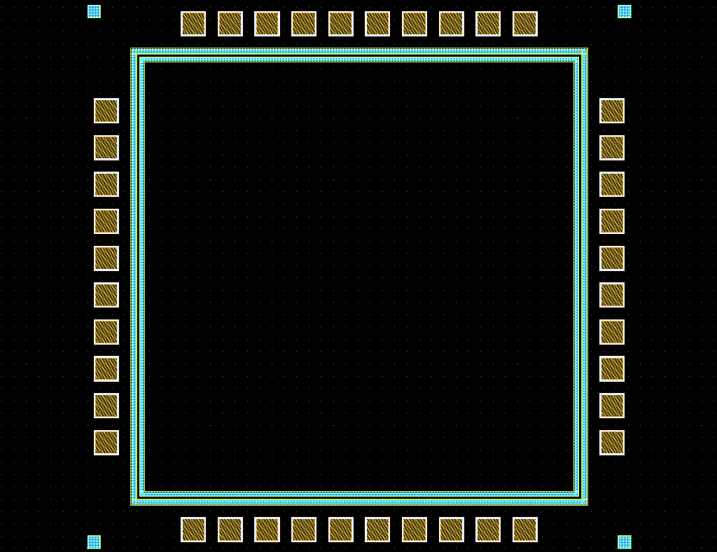
Initially it was 8 packaged and 32 unpackaged chips:
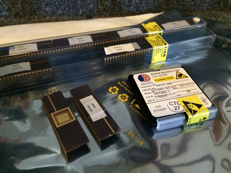
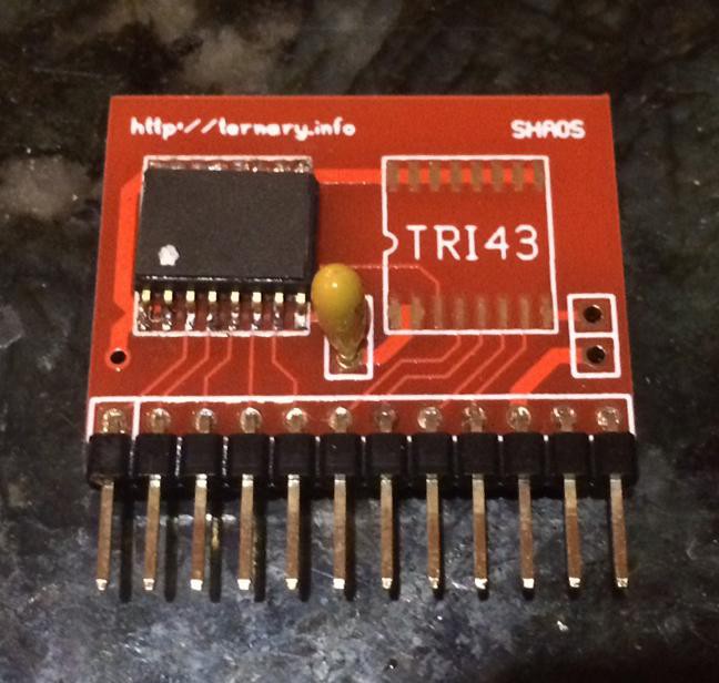
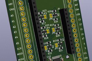
Later I packaged all unpackaged dies and got 3 different packages for the same die - DIP40, DIP28 and SOIC16:
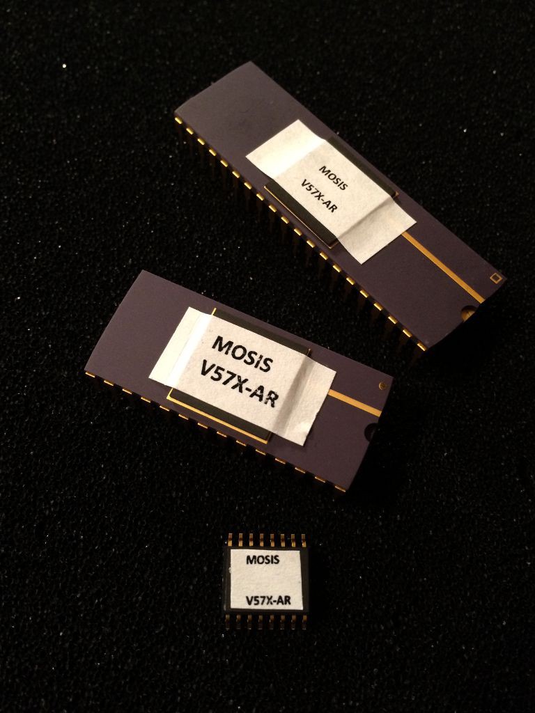
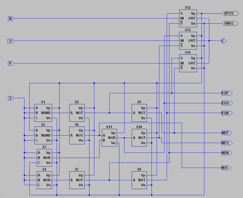
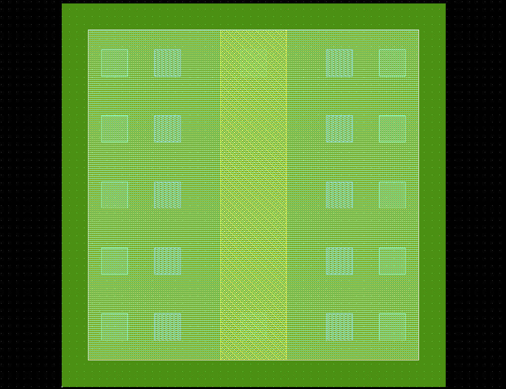
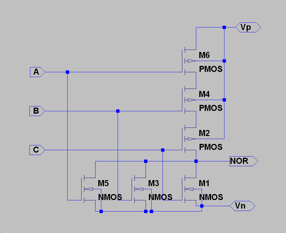
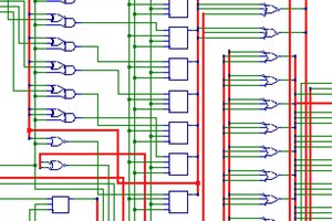
Chip itself is 3 separate test projects on one silicon die:
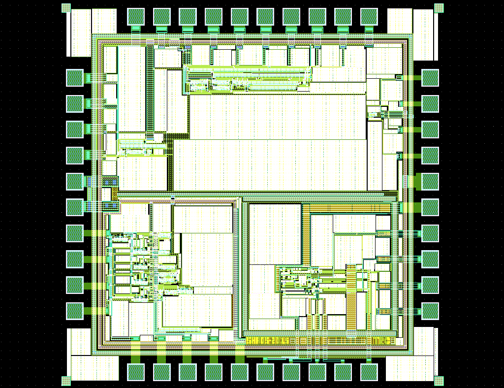
Each test project is a collection of CMOS circuits to test basic building blocks for binary, ternary and quaternary logic. Work was done in conjunction with a stealth hardware start-up that will reveal more details soon...
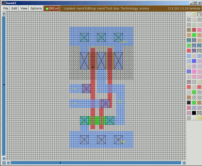
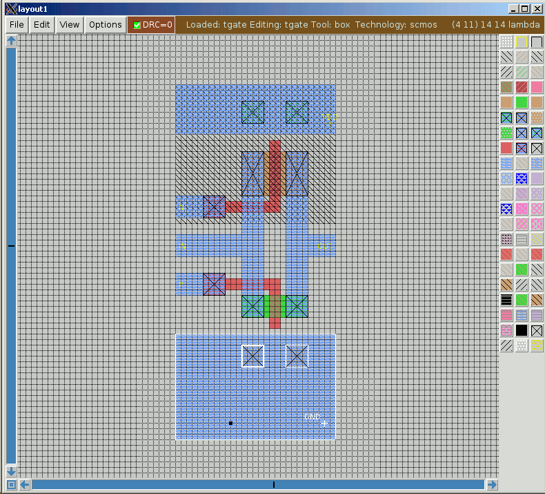
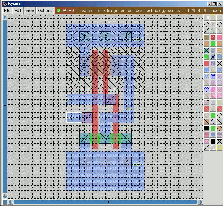
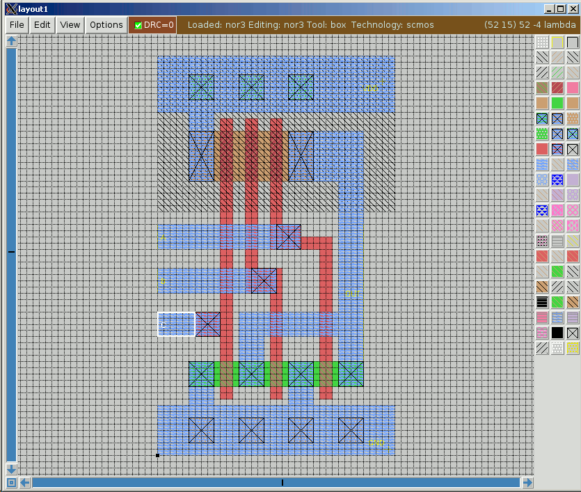
Magic VLSI layout open source tool: http://opencircuitdesign.com/magic/
Technology files for Magic: http://opencircuitdesign.com/magic/tech.html
We use SCN3M.35 technology (0.5um lambda=0.35).
To run Magic with this technology files:
magic -T SCN3M.35
Below you can see very helpful Magic tutorial from Youtube user CellRider:
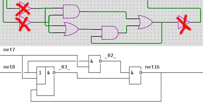

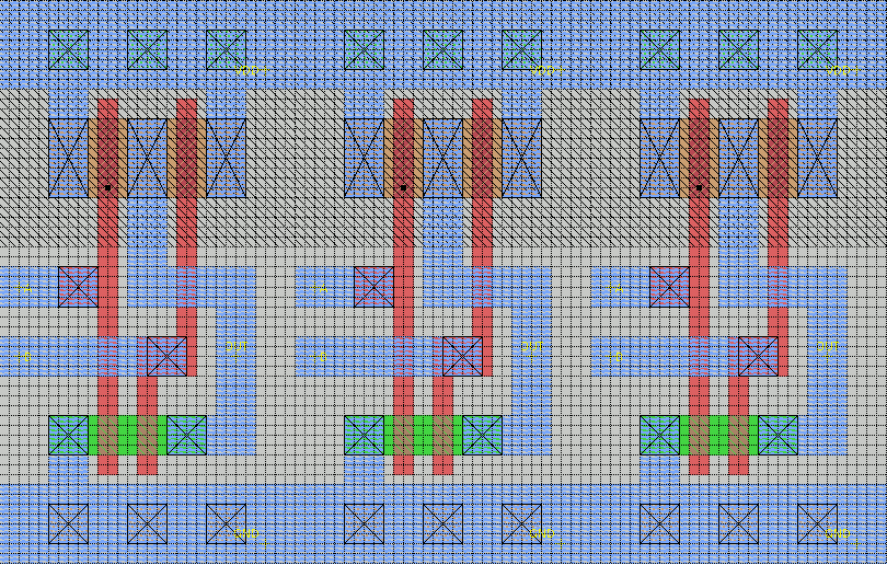
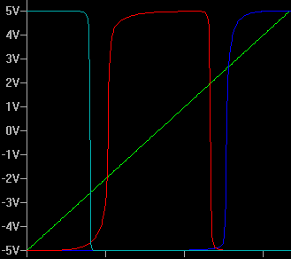
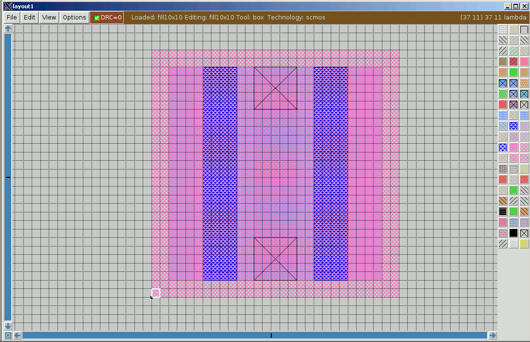
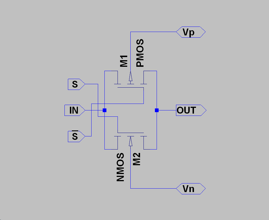
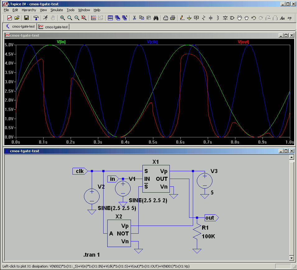
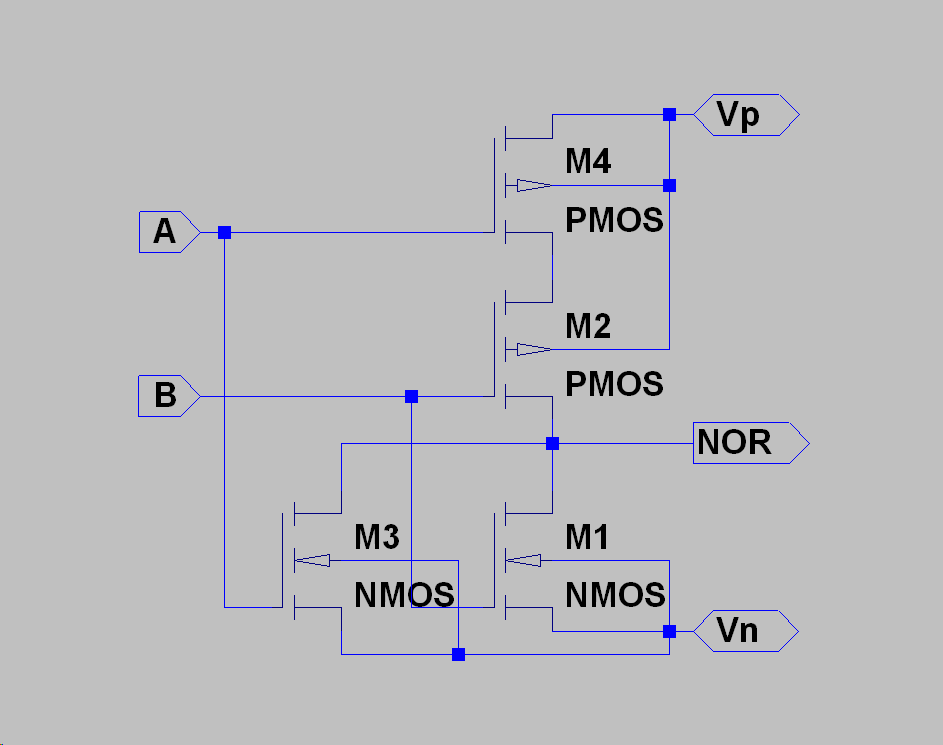
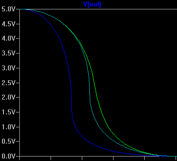
 So one ternary selector has:


 Yann Guidon / YGDES
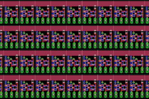
 Duane Thompson
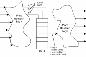
https://hackaday.com/2023/03/05/tiny-tapeout-3-get-your-own-chip-deign-to-a-fab/