-
[CWM2] Done (for now)
04/03/2015 at 23:13 • 0 commentsA few landing prints and components have been replaced depending on what is more readily available at the moment. Also more indication lights have been added to put all of the remaining IOs of the ESP8266 to good use.
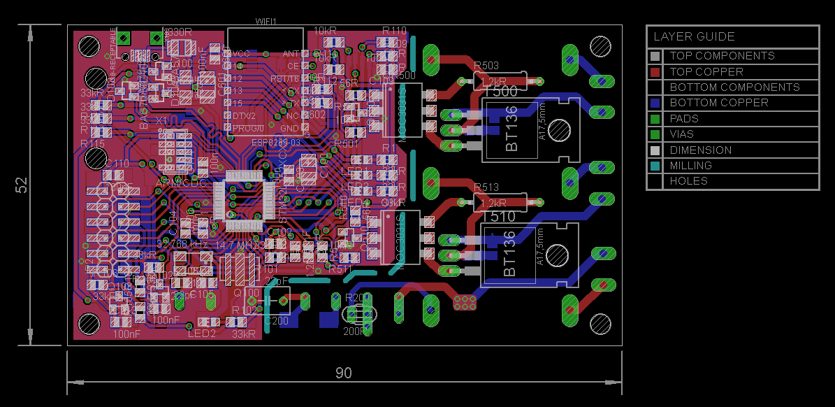
The only thing making me nervous now are the clearances on the primary side.
Well, at least the DRC checked out without a hunch.
Edits:- Removed Denglish
- Forgot to Ratsnest before exporting image
-
[CWM2] It's getting somewhere
04/01/2015 at 04:10 • 0 commentsLots of packages were swapped. Connectors rotated, moved, rotated, then put back.
Fun stuff, for now.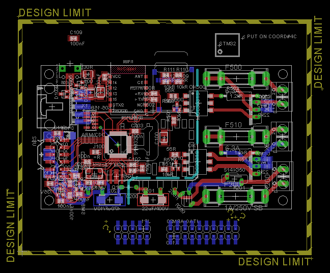
Seen on the right lies the almost finished mains management, as indicated by the milling for bumping up the creepage distance.
This area consists of two triac-based AC switching units, tested to switch up to 800W at 230VAC combined with MOC3031S optocouples to drive those.
In the bottom left corner the input protection circuitry for the switch-mode converter can be found. In theory this should protect against all kinds of troubles later, given I implemented the application note correctly.
The secondary side consists of an ARM Cortex M0, various interfaces and of course the famous ESP8266.
Of course there are still serious issues with the current layout like general part clearances and trace widths on the primary sides, but I am positive those will be gone soon. -
[CWM2] It begins ...
03/31/2015 at 00:20 • 0 comments94 parts, 20 hours in, limited board size.
Hopefully reaching the Holy Grail of PCB design once again.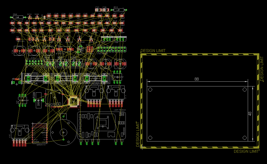
This user joined on 12/14/2014.
 The Big One
 zakqwy
 ThunderSqueak
 Voja Antonic
 jaromir.sukuba
 baoshi
 Ben Krasnow
 Bruce Land
 Welsh Mullet
 Pengu MC
 doctek
 Zack Sutphin
 martin
 naqua
naqua filid
filid