-
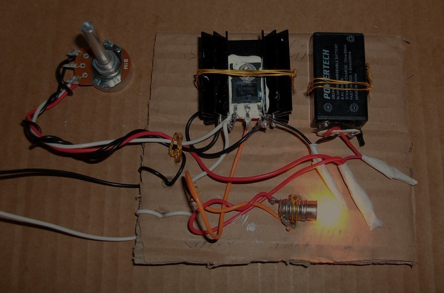
MOSFET Sensor Amplifier
11/10/2020 at 07:46 • 0 commentsThis article shows a simple n-channel MOSFET sensor amplifier.
The sensor output is could be either a biased/non-biased sensor or a pre-amplifier amplifier output.
The power MOSFET that I used is also able to drive high power/current loads (bright LEDs/light bulbs/motors/relays).
The 1 Megohm potentiometer provides a variable voltage divider source to the MOSFET gate pin. As soon as the MOSFET gate voltage reaches a specific minimum threshold, the MOSFET turns ON and provides current to the load that is connected to the MOSFET drain pin. The source of the n-channel MOSFET is grounded or connected to a negative battery lead.
![]()
The potentiometer can be adjusted just on the edge of triggering which will allow non-linear but reasonably high amplification of changes in sensor output voltages.
You can see in my circuit that the sensor output (white wire) is connected to the MOSFET gate via 10 kohm resistor to ensure that the potentiometer does not short the sensor output when it is set to zero MOSFET gate voltage.
Calculations for selecting a heat sink are explained in this link:
https://www.instructables.com/Component-Heat-Dissipation
1. Videos
Tuning:
I connected the input to my signal generator:
2. Testing
I used a 12 V light bulb and 9 V battery believing that my power MOSFET could handle the 9 V maximum gate pin voltage.
Night time photo:
![]()
I connected the input to the signal generator and increased the frequency:
3. Conclusion
A significant amplification might be required before the sensor output signal enters my MOSFET circuit to achieve a proper sensitivity of the sensor circuit.
-
Biased Sensor Bridge
10/30/2020 at 00:22 • 0 commentsThis article is showing a biased sensor bridge.
A more expensive sensor bridge that allowing biasing polarity changing is explained here:
https://www.instructables.com/Biased-Sensor-Bridge/
A cheaper unbiased sensor bridge is shown here:
https://hackaday.io/page/9364-unbiased-sensor-biasing
Step 1: Design the Circuit
I drawn the circuit in PSpice simulation software.
![]()
I used Rs1 and Cs to filter power supply oscillations. I also used Rs2 to limit that maximum sensor biasing current.
Step 2: Simulations
Simulations show the differences in output voltages:
![]()
-
DC Transistor Amplifier
10/16/2020 at 00:01 • 0 commentsThis article is about two different DC transistor amplifiers:
![]()
The only difference between two amplifiers is the difference between Rc1a and Rc1b resistors. Those resistors ensure that the amplifier output is not random when the Q2a and Q2b transistors are disconnected. This occurs when the Q1a or Q1b collect voltages are equal to the power supply voltage. The Rc1a and Rc1b resistors keep the Q2a and Q2b transistors OFF.
If you would think that Rc1a and Rc1b will have no affect on the output value, then the simulations will show how wrong you are. Rc1a is 10 times more than Rb2a in value. If we do the calculations for the Q1a transistor load then you will find that Rc1a will increase the load and the Q1a transistor, increase the collector current and reducing the load resistance. The Rc1b value that is 100 times more than Rb2b resistor will have less influence on the amplifier gain.
We are assuming that both transistors are biased at half the power supply voltage.
The Q1a load resistance equals to:
RcA = Rc1a || (Rb2a + Beta*re)
= 10,000 ohms || (1,000 ohms + 100 * 0.026 / IeA)
IeA = ((Vs / 2 - Vbe2) / Rb2a + Vs / 2 / Rc1a) / Beta * (Beta + 1)
IeA = 0.0009595 = 0.9595 mA
= 10,000 ohms || (1,000 ohms + 2,709.74465868 ohms)
= 2,705.91812688 ohms
The Q1b load resistance equals to:
RcB = Rc1a || (Rb2a + Beta*re)
= 100,000 ohms || (1,000 ohms + 100 * 0.026 / IeB)
IeB = ((Vs / 2 - Vbe2) / Rb2b + Vs / 2 / Rc1b) / Beta * (Beta + 1)
IeB = 0.00082315 = 0.82315 mA
= 100,000 ohms || (1,000 ohms + 3,158.5980684 ohms)
= 3,992.56340381 ohms
The output voltage is the product (multiplication) of collector resistors (Rc1a or Rc1b) and collector current (Ic1a or Ic1b). Thus increasing the load resistances (Rc1a or Rc1b) might increase the amplifier gain. However, increasing the load resistances (Rc1a or Rc1b) will also reduce the biasing current (Ib1a or Ib1b) and thus the transistor current gain as well that will reduce the collector current (Ic1a or Ic1b).
Simulations
PSpice simulations show the difference in output voltages:
![]()
The first amplifier has a higher voltage gain. However, this could be due to current gain differences. By changing the current gain characteristics of each transistor you might be able to increase the current gain of the second amplifier.
My Pages


Projects I Like & Follow
 Lutetium
 bobricius
 M.daSilva
 Shane Burrell
 Ulrich
 Kelly Heaton
 Ates Goral
An ATtiny Annoy-O-Tron with a Hewlett Packard Colorado T100E Tape Backup Drive. What!?
 Pete Prodoehl
 Rahul Khanna
 igorfonseca83
 Roni Bandini
 Jason Cho