-
Uncovering the World of Graphic Overlays
09/29/2023 at 02:49 • 0 commentsThe recent increase in availability of creator tools and services over the past few years has allowed many low-risk entry points for hobbyists, amateur product developers, and DIYers of all backgrounds to crack the often-mysterious seal surrounding hardware development. Some of these tools include free schematic software, free layout software, free 3D CAD software, low-cost PCBs, low-cost PCB assembly, low-cost 3D printing, and easy access to online component distribution. With a little bit of YouTube searching, tutorial watching, and mental elbow grease, any motivated hobbyist can crank out professional looking circuit boards and housings for their projects. This can then allow amateur innovators to do small batch production and early product testing, all without needing access to large amounts of capital for professional product development.
An often-overlooked service in this category of low-cost prototyping is custom graphic overlays. Graphic overlays and acrylic panels consist of a piece of durable material, printed graphics (button labels, logos, etc), transparent windows for displays, holes for buttons and connectors, and adhesive to adhere to a housing. A graphic overlay can allow for a concise user interface and protection of displays while also providing professional polish to a product. My experiences with creating graphic overlays over the past few months has allowed me to add this extra tool into my prototyping toolbelt. Very few tutorials or guides were found online, so this post serves as an entry point and call to action for anyone out there who could find value in a description of the graphic overlay creation process I experienced.
The process to create an overlay or acrylic panel consists of defining the product housing, defining the overlay outline, defining the overlay graphics, creating the design documentation, and submitting the order. The next few sections will describe the general process used to complete each of these steps.
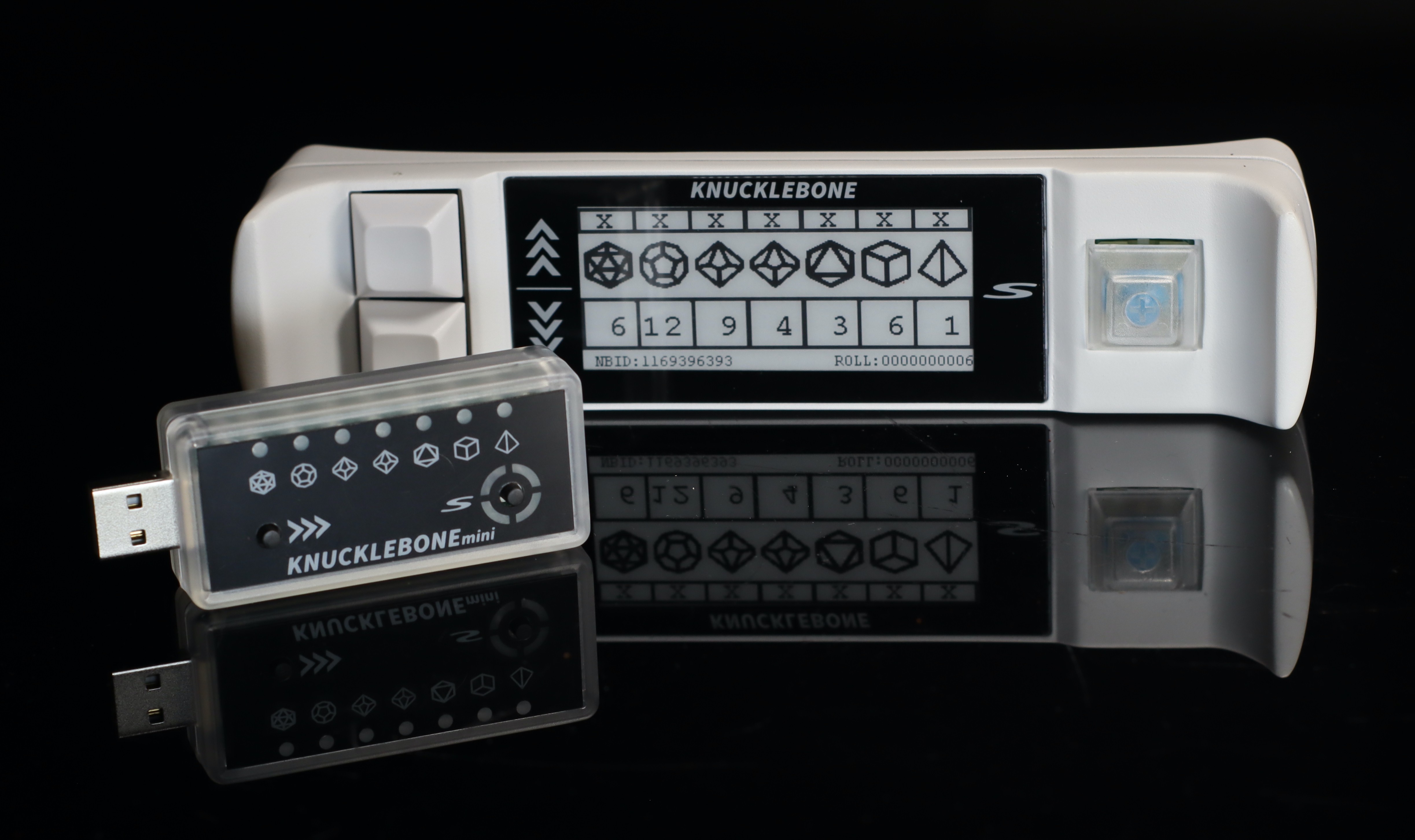
Image below depicts a recent electronic dice Kickstarter project using graphic overlays and acrylic panels:
![]()
Define the product housing:
There are two common options to consider when deciding what to use to house your PCB and electronics: a custom 3D CAD housing design or an off-the-shelf housing.
Off-the-shelf housing design:
An off-the-shelf housing design is a very attractive option when in the early stages of prototyping, product viability testing, or low volume productions. Off-the-shelf housings allow developers to minimize design time and minimize prototyping costs. Hammond Manufacturing and Bud Industries are examples of two companies that provide durable readily available housings in a variety of form factors. They also provide custom modifications to the housings as requested. These housings can easily be pulled into a 3D CAD software (e.g. Fusion360) where any cutouts can be defined.
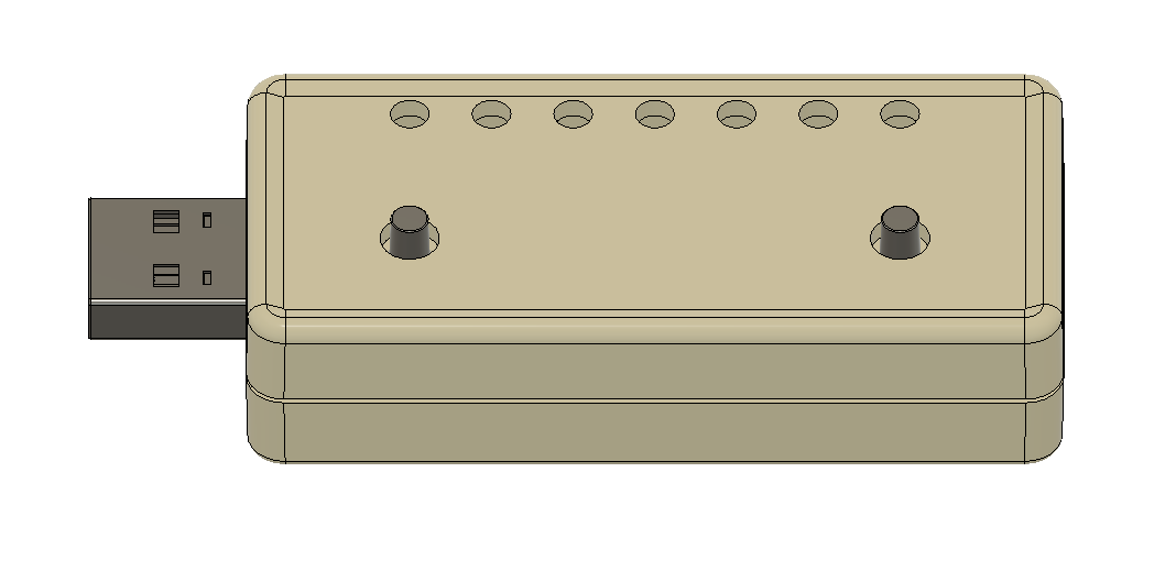
Image below depicts a KnuckleboneMini housing design utilizing an off-the-shelf Hammond Manufacturing enclosure. LED holes and button holes are shown:
![]()
Custom 3D CAD housing design:
A custom 3D CAD housing design is a good option if the function or styling of the device demands a unique shape. It is also a good option if the device may be injected molded for high volume production in the future. A custom 3D housing design does incure additional development time. It also will require 3D printing services (e.g. Unionfab or Xometry) for prototyping.
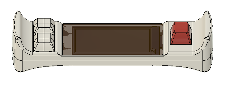
Image below depicts a Knucklebone housing design utilizing a custom 3D CAD enclosure design. The ePaper display can be seen modeled below the acrylic panel component so that precise location of the transparent window in the acrylic panel design is possible:
![]()
Regardless of the housing design method chosen, it is critical to identify where...
Read more »
This user joined on 09/29/2023.
My Pages
Things I've Built
Nixie Clock and Speaker
A custom nixie clock with 6 numerical tubes, a bar graph, and an audio amplifier tied together in a custom acrylic housing.
Fresnel Clock
An old small wrist watch becomes a wall clock with the help of a fresnel lens.
Fish Tube
A tubular fish tank made out of acrylic tubing and aluminum intake tubes! Also includes hidden lighting, filter, and aerator.
 Julian Fernandez
 Ryan Kinnett
 Scoops
 Nikhil Mishra
 Luke Brandon
 Sean
Sean Andrea Console
 mircemk
 Ralph
Ralph kutluhan_aktar
 CircuitMonster
 MWK
MWK kadugarcia
 Sagar 001