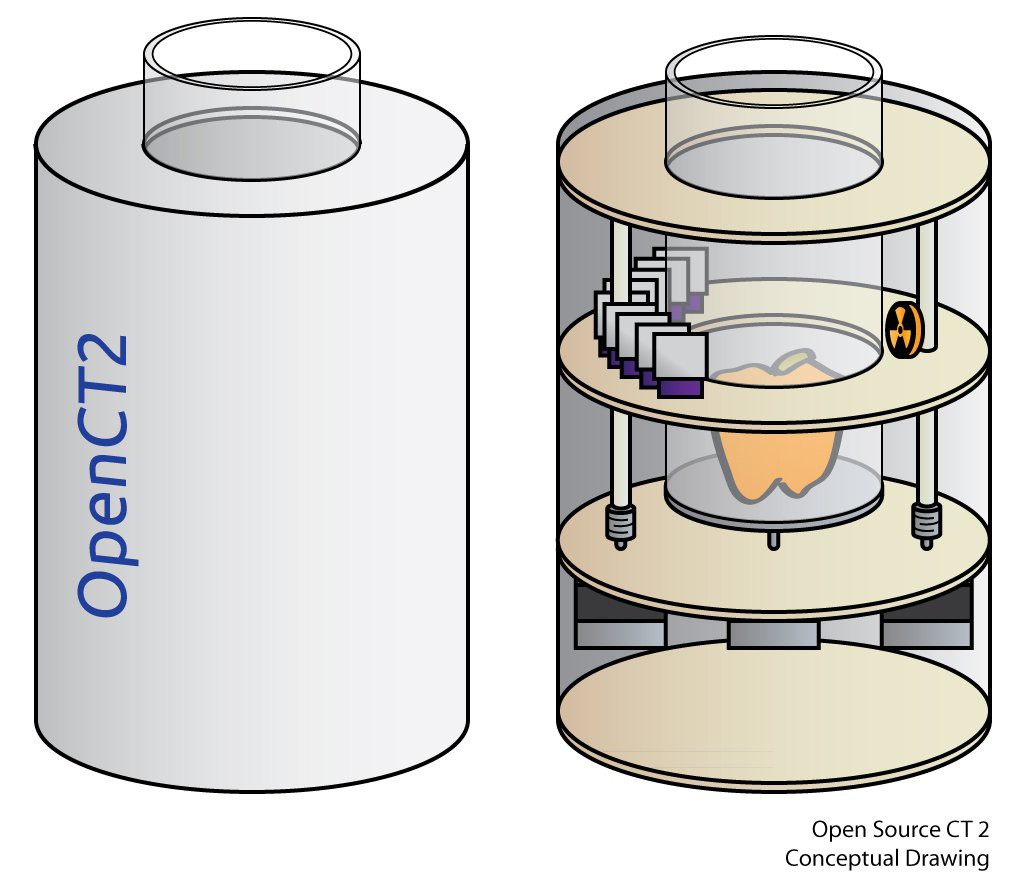
Close
0%
0%

OpenCT2

An open source low-resolution desktop CT scanner

Similar projects worth following
Harness the power of the atom to scan inside objects with this nuclear powered desktop volumetric computed tomography (CT) scanner!

Summary

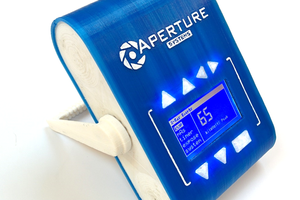
Last year I designed the first iteration of an open source computed tomography (CT) scanner. It was a lot of fun to design, having many atypical design problems in it, from the mechanical design of the rotary gantry to pairing an appropriate radioisotope source with a modified extra-sensitive radiation sensor. Something about it being essentially a radioactive desktop Stargate that lets you see inside of things also seems to get people very excited, and so I've received an eclectic bunch of e-mails asking about the scanner from folks as diverse as radiology professors and biomedical folks to makers to those hoping I'd open up Dr. Jansen's back-alley CT scans to have a look at some strange bump they have (please go see your doctor!).

But I feel that for all the excitement, to quote Feynman, that first open CT design feels a bit like a dog that walks on two legs — it's not that it does it well, it's that it does it at all that gets people excited. It's essentially a working model of the first generation of CT scanners, but with a much weaker source, and so it takes a very long time to get even a single slice of an image. I've been wondering what it would take to move the idea of a desktop CT scanner from a proof of concept into something that does the job well, or at least substantially better.

OpenCT2

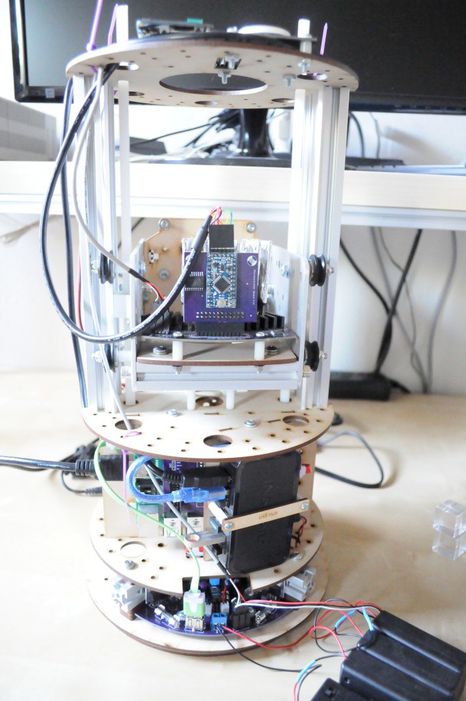
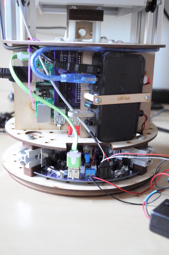
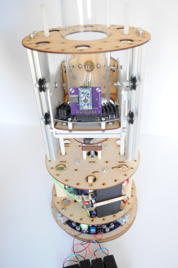
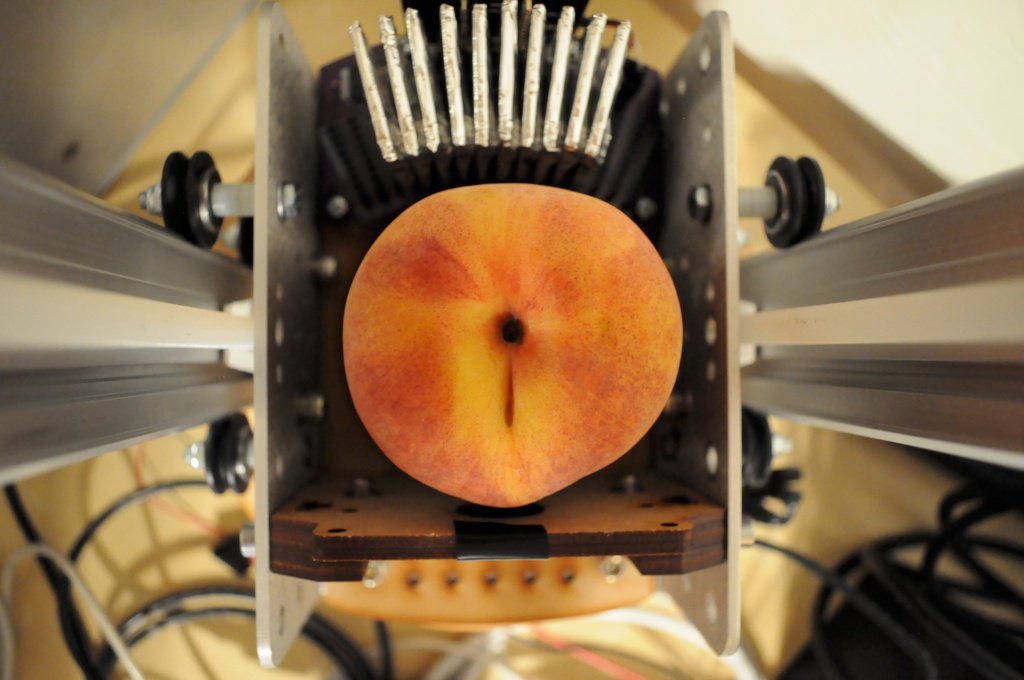
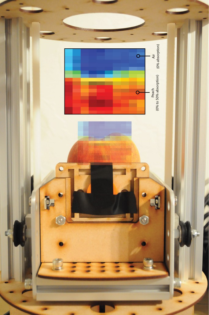
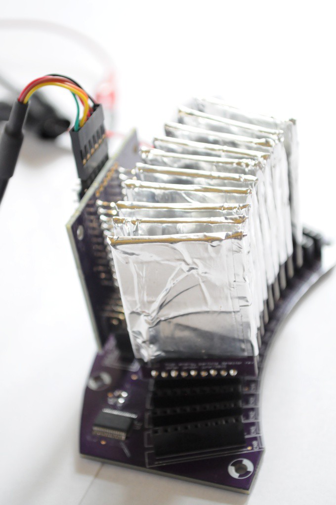
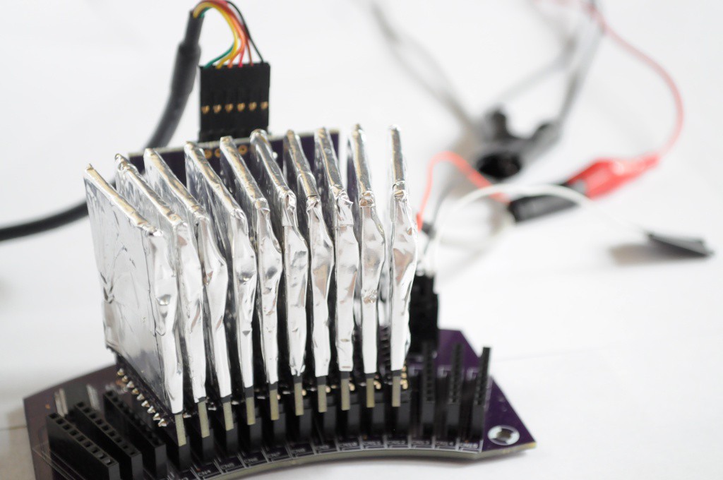
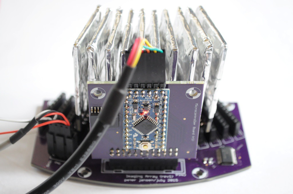
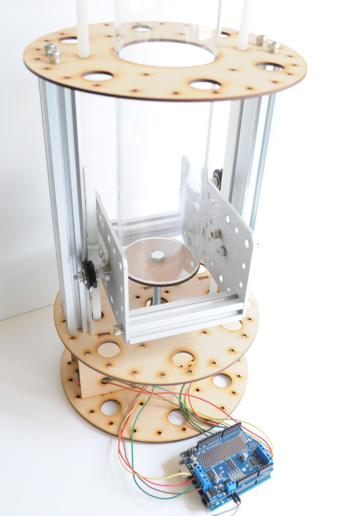
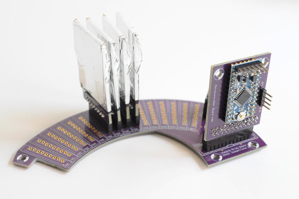
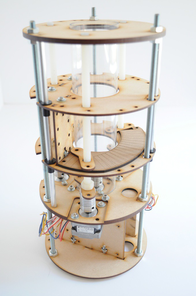
The OpenCT2 is my attempt to move the design much closer to the tomographic systems in use today, and make a complete third generation desktop CT scanner that uses a large parallel array of detectors. This should decrease the acquisition time substantially, acquiring low-resolution images on the order of an hour, and tomographic scan times on the order of a day.

Design Goals and Constraints

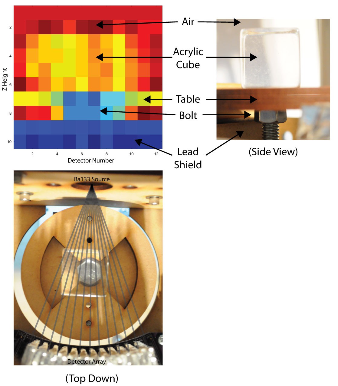
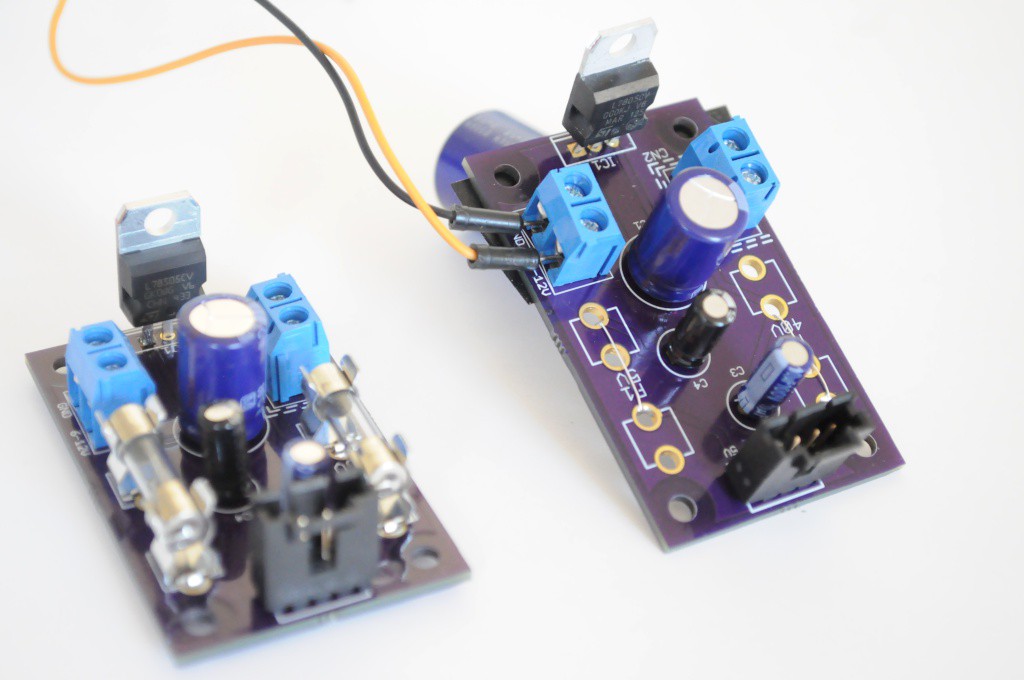
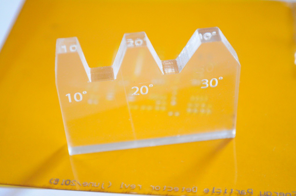
  • Extremely low intensity source: Instead of using an x-ray tube, for safety the system is designed to use a low-intensity radioisotope source. The 10uCi Barium-133 source used with this system is the most intense radioisotope source that one can purchase without a license in the US. This constraint makes the design much safer than using an x-ray tube, but it's also the major limiting factor in acquisition time -- because the source is of such a low intensity, the acquisition times are essentially bound by the shot noise associated with photon counting. For those professionals extremely well trained in radiographic safety, with appropriate lab facilities and comfortable modifying open designs, it should in principle be possible to mount a small x-ray tube in the design, decreasing scan times from the order of a day to a few minutes.
  • Compact, and in it for the long haul: The design should be small, self-contained, and attractively fit on the edge of ones desk. The scan times are limited by physics and safety.
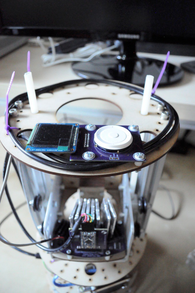
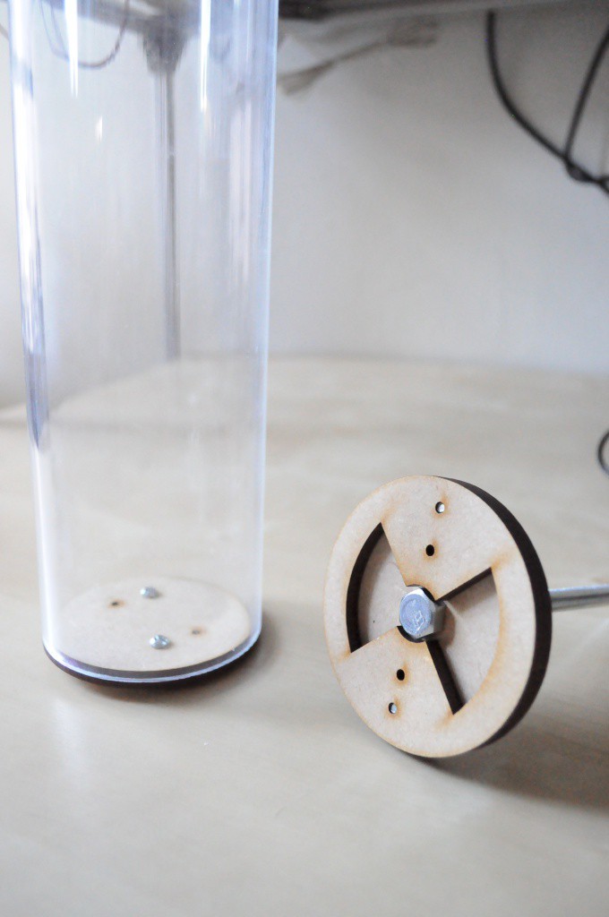
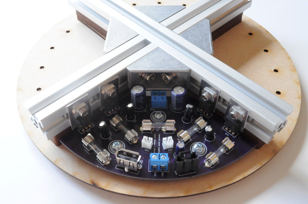
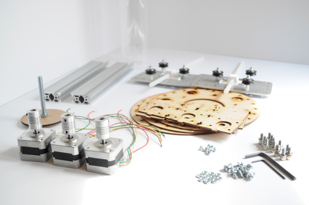
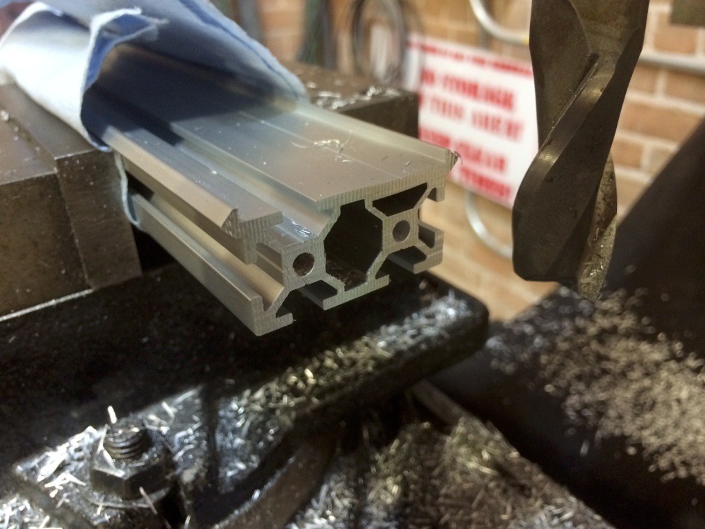
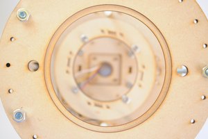
  • Mechanically simple: The tomographic platform is designed to make use of a simple rotating sample tube and single linear axis, instead of a complex rotating gantry.
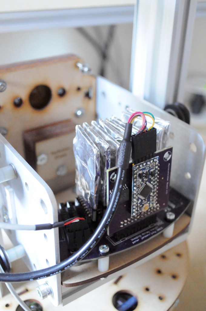
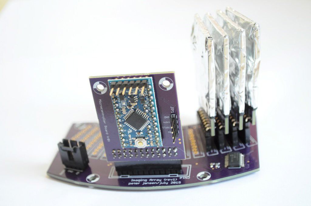
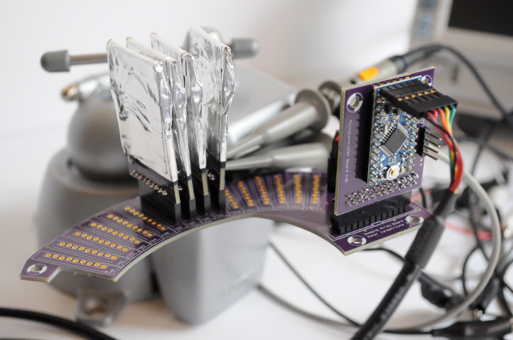
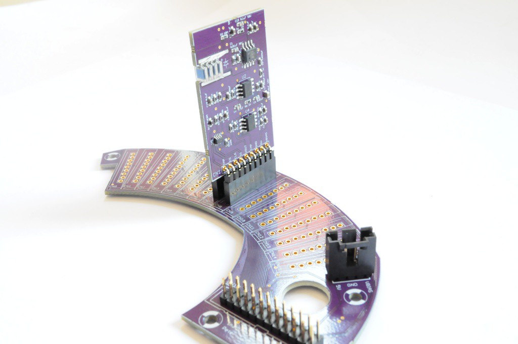
  • Modular: The three main components of the system (radiation sensors, imaging array, and tomographic platform) are modular -- so whether you're simply looking for a design for an inexpensive high-energy particle detector, or a tomographic platform to mount your infrared or terahertz system upon, there's something for scientists and engineers of many interests.
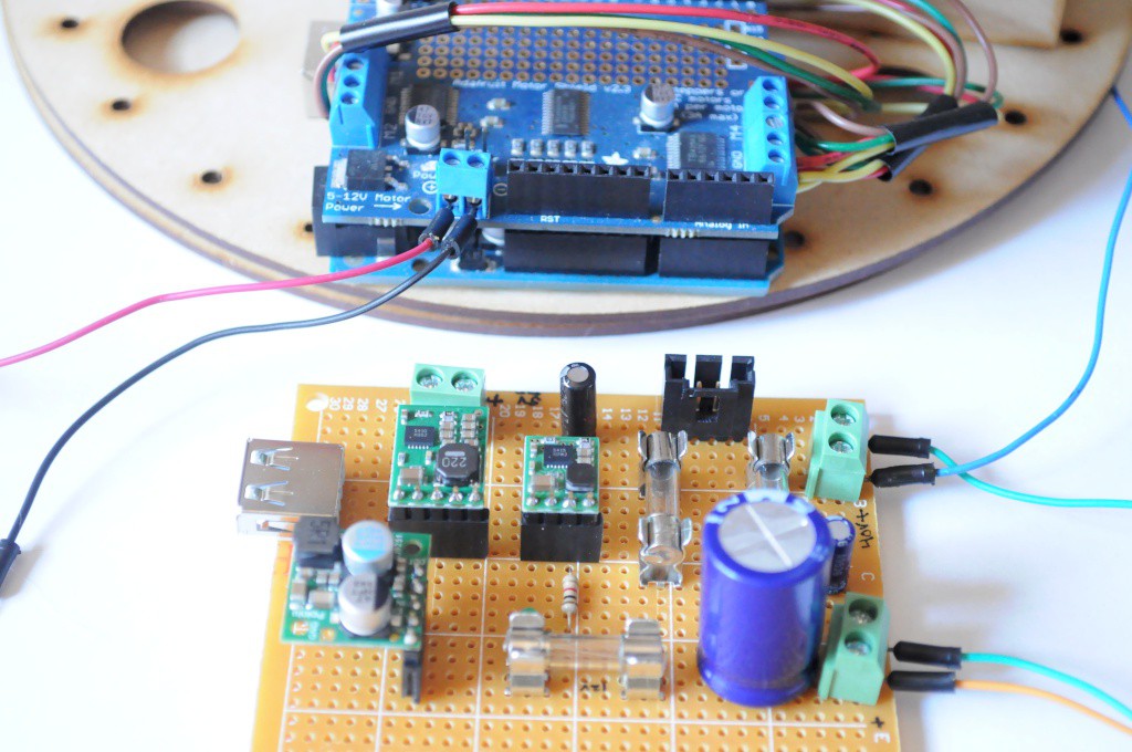
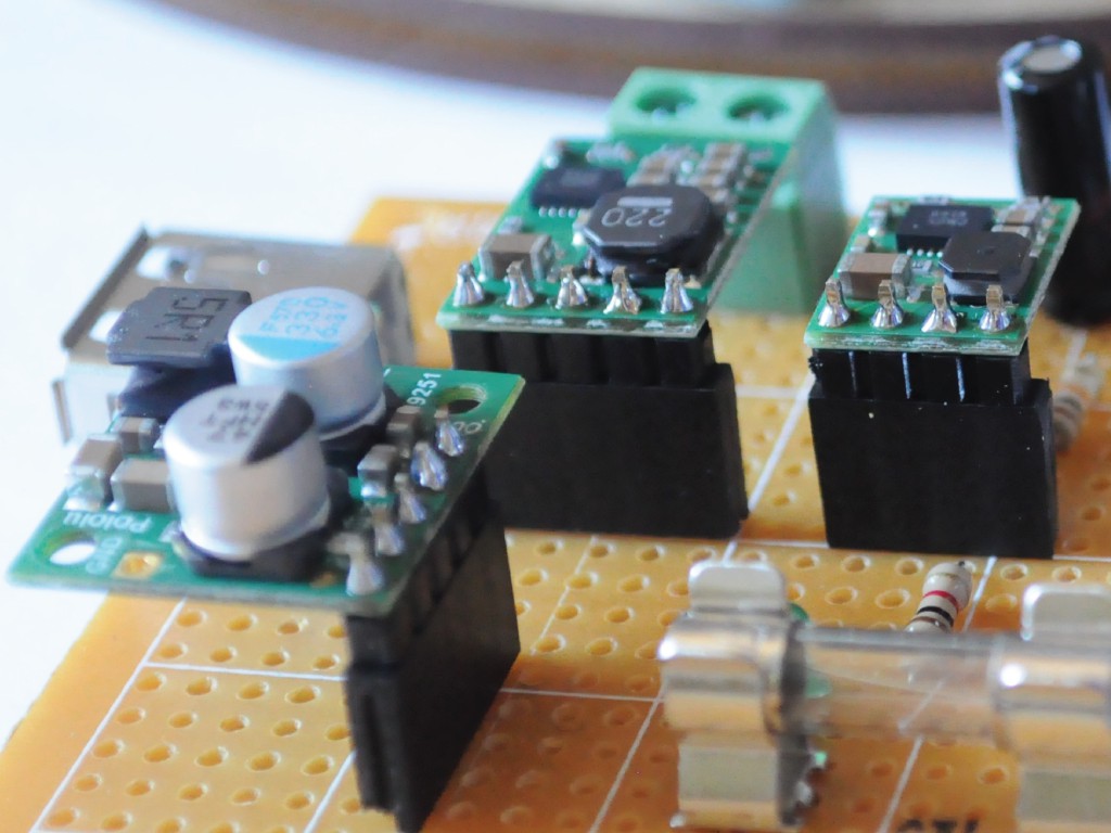
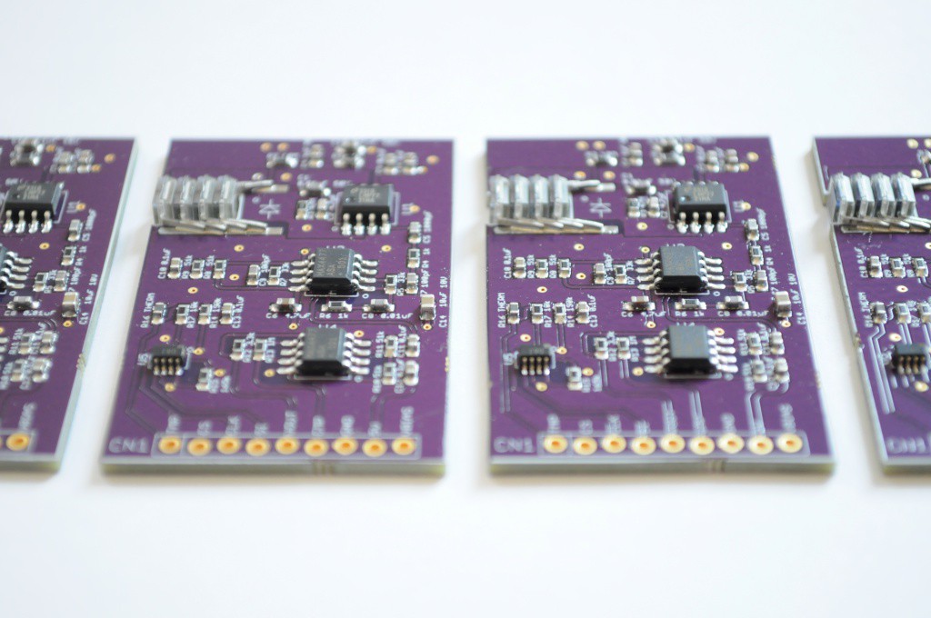
  • Easy to assemble: The system is being designed to be capable of being assembled by a keen undergraduate with modest surface mount assembly skills. The modular detectors generally make use of SOIC ICs and 0603 passives. To make the tomographic platform as general as possible, it's designed to be assembled using largely off-the-shelf components, and basic through-hole soldering skills.

Contributions

The project has three main contributions:

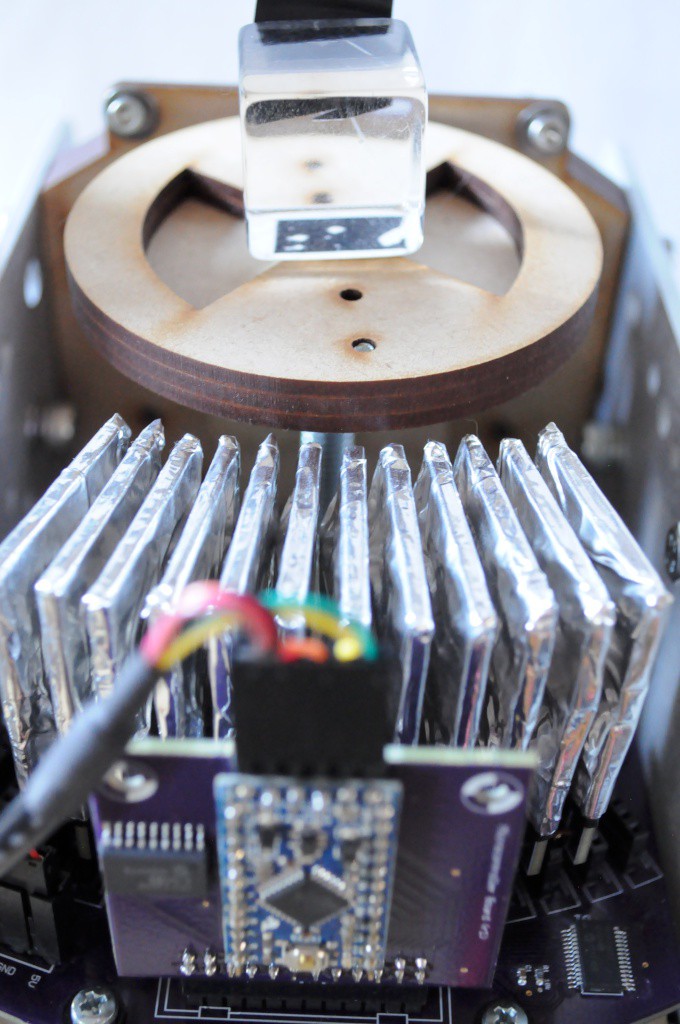
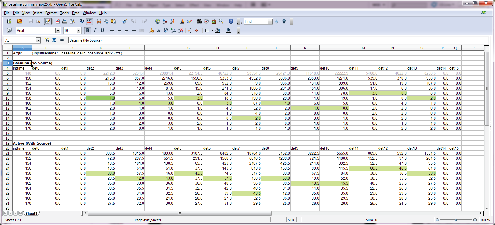
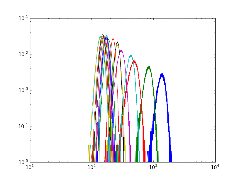
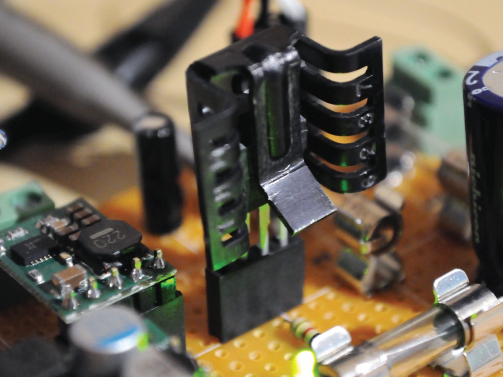
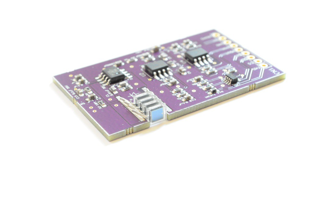
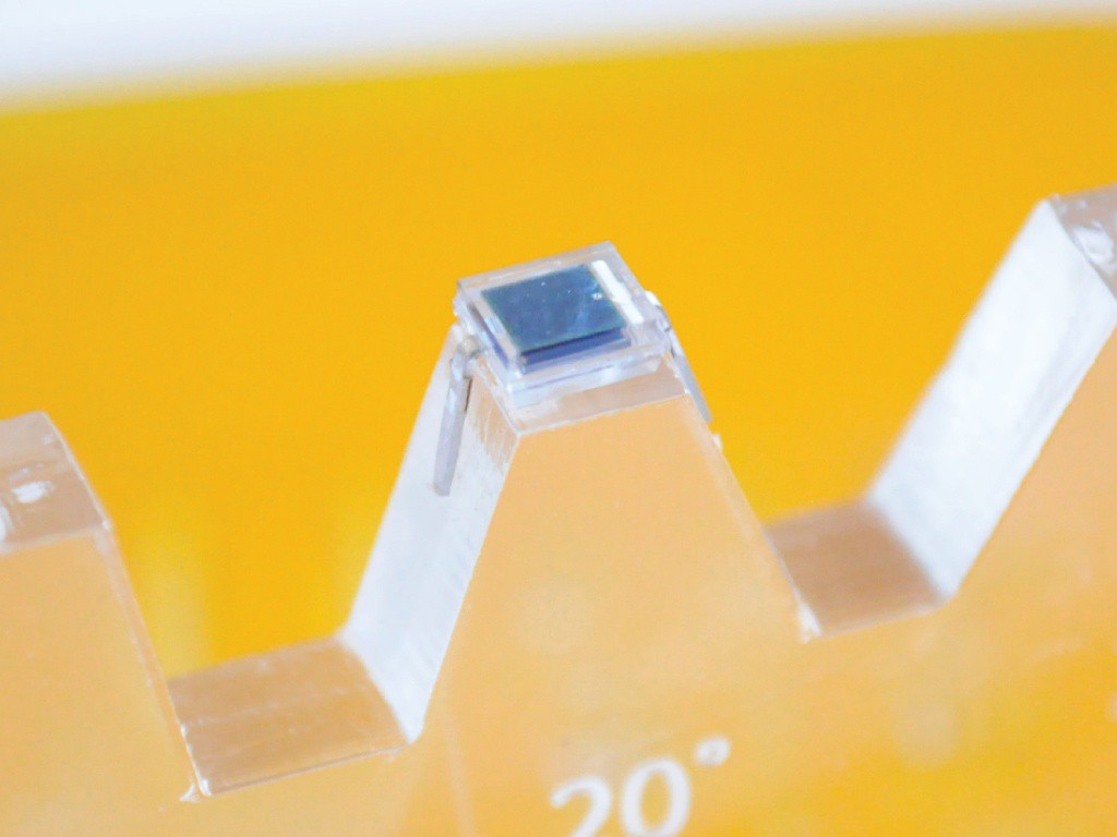
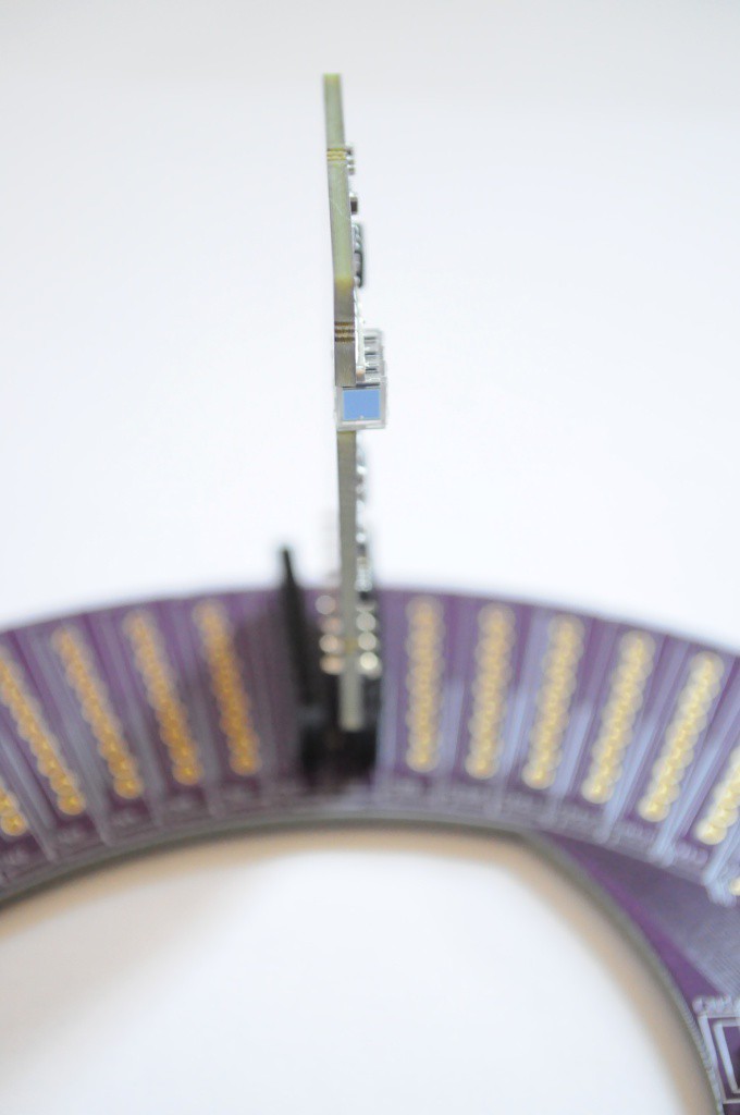
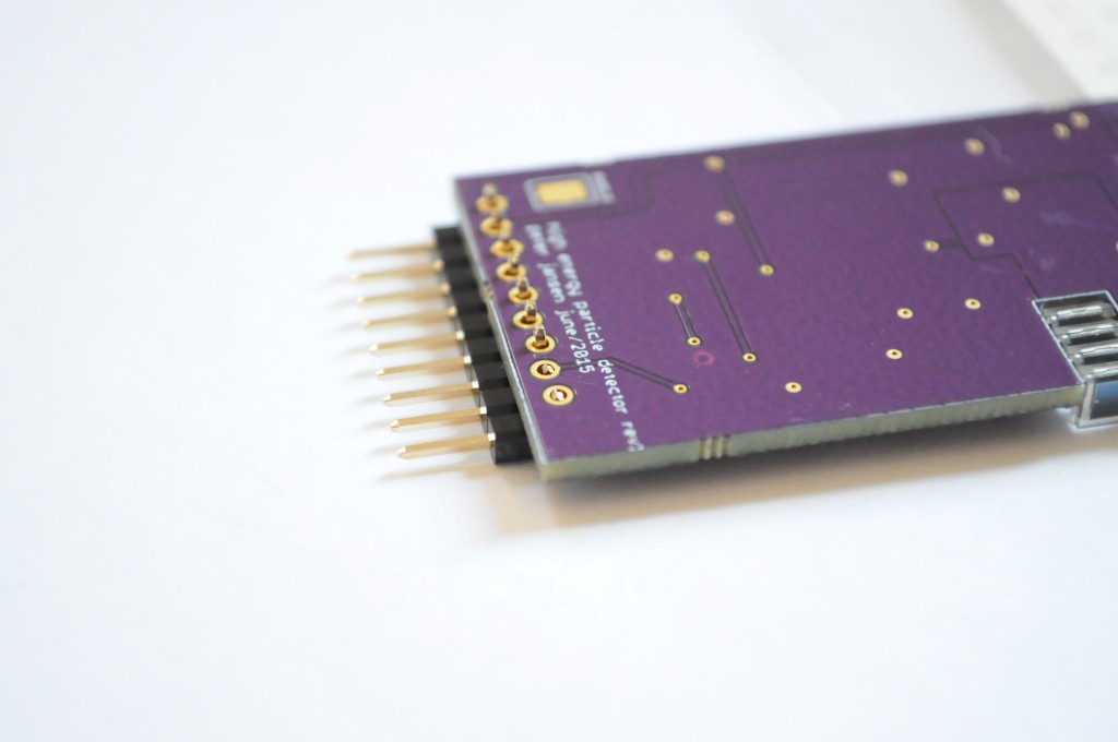
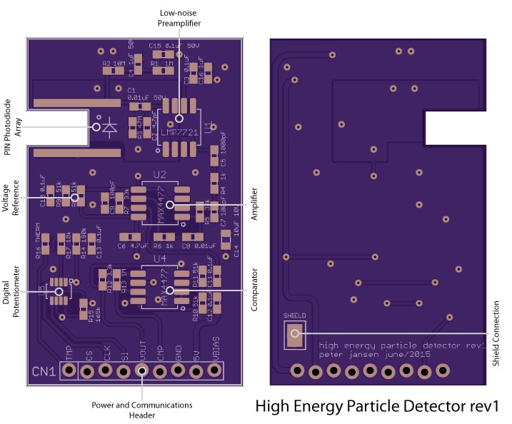
  1. An inexpensive modular radiation sensor suitable for low-resolution spatial imaging (nearing completion). These modules have pixel sizes of about 2.5mm square (7.5mm^2 area), and are designed to be placed in close proximity to form one dimensional imaging arrays. The single-quantity BOM for...
Read more »

  • The first tomographic reconstruction!

    peter jansen05/05/2016 at 05:10 2 comments

    After building and populating four more detectors, the array had 12 pixels total, which sounded like enough to try to capture an image, and then move on to capturing the first tomographic slice. Here, I'll show an absorption image of an acrylic cube, show the calibration data, then collect and reconstruct the first tomographic image!

    First, a (non-tomographic) x-ray absorption image

    I decided to try to use a small acrylic cube as a test article, because acrylic appears reasonably absorptive to x-rays, and unlike the fruit and vegetables that I've been scanning, it doesn't decay. Above is an image constructed by measuring the absorption along 10 positions on the Z (up/down) axis, over about 50mm/2 inches of height. Here, on the bottom of the image, we can clearly see several features:

    • Starting from the bottom, the lead shield, which blocks most of the high energy particles travelling from the Ba133 source towards the detectors, when the Z axis is at the lowest (homed) position. (High absorption, blue)
    • Next, the metal M8 bolt used as a shaft for the sample table. (High absorption, blue)
    • The MDF sample table (Medium absorption, yellow). The bolt is visible through the middle of the MDF (blue)
    • The acrylic cube (low (red) to medium (yellow) absorption, depending on how much acrylic a given emission path has to travel through on the way to the detector)
    • Air, at the top (very low absorption -- red).

    All the important elements (shield, bolt, table, acrylic, air) are clearly visible and easily differentiated. The image might look a little unusual because (a) it's measuring absorption (like density) instead of the amount of light a given location is reflecting back, and (b) the image plane is cylindrical rather than flat, so that the distance from the source to each pixel on the detector array is constant -- so it's like the opposite curvature of a fish-eye lens.

    A very successful image. Above, because of the extremely low intensity source, each pixel is the aggregate of about 15 minutes of exposure. The long integration time is to get a rough estimate of the actual absorption given the high rate of shot noise, which (at this integration time) appears to be in the neighbourhood of +/-20% -- so still quite large, but not impossibly so.

    Above is a picture of the 12 detector array, which is four more detectors than have been previously populated. 4 detectors (2 on either side) still remain unpopulated.Calibration

    In spite of using some of the most precise opamps and high tolerance passives that are available, to my surprise, there is still a good deal of individual variation in the noise levels between each of the 12 detectors. This is a very important result, and answers a question I'd often had about the fantastic Radiation Watch Type 5 detector, used in the first OpenCT -- the detector is capable of detecting much lower energy levels by changing a single resistor value on the comparator, so why did they set the threshold so much higher? The answer is that setting the threshold very conservatively likely increases the manufacturing yield -- with the possibility for so much variation between units, the designer likely chose a safe value to ensure that >99% of their detectors would pass the QA process, at the expense of many of those detectors being less sensitive than they may ultimately capable of being.

    By including the digital potentiometer in my design, I ensure that the detection threshold of each detector can be individually tuned to just above it's noise threshold, ensuring that each detector is at peak efficiency. From the cable of counts (above) for each of the 12 detectors at 10 different digipot settings, one can see that a uniform safe resistor value might have had the efficiency of each detector lowered by between 10-50%, meaning significantly longer integration times for the same signal. A definite win, when working at the extremely low signal-to-noise ratio of this system.

    Ba133 emits over a wide range of energies, and the detector likely...

    Read more »

  • A table, a radiation shield, and making everything fit

    peter jansen04/03/2016 at 20:34 1 comment

    A quick update with nearly-complete mechanical progress (!), including creating the table, and the radiation shield used for calibrating the detectors. The focus here has been on having the unit completely self-contained, so it can do long calibration procedures (featured in the next post), and of course scanning procedures.

    The (nearly complete) unit, on the workbench. Though it looks very similar to the last revision, nearly every piece has been modified with mechanical considerations for cabling, assembly, and having the entire unit self contained within an 8-inch cylinder (so that a case can be designed to slide over it, and look attractive on one's desk).

    Here, the cables for the two Arduinos (one on the imaging array, the other to control the linear and rotational stages) are finally securely mounted and plugged into the USB hub. The remaining positions in the hub include:

    • A 16GB USB flash drive, which hosts the Raspberry Pi filesystem. This is used in lieu of the traditional SD card in that it's both faster, and seemingly much more resistant to being corrupted.
    • A Wifi module, for headless operation. Much of the software that I've been writing has been developed on the machine itself, using a remote desktop over VNC.
    • USB Keyboard and Mouse

    The HDMI connection to the Raspberry Pi is also visible on the left. One of the final mechanical considerations is to laser cut a plate for the back of the machine that breaks out the HDMI, one USB, and the power connector, and to find short panel-mount extension tables for these ports.

    Because the development environment is notoriously hostile to parts, I'd populated the imaging array with only two detectors for testing, so that if something accidentally bridged, at worst only two of the detectors would be damaged. While the detectors have been designed to have a low bill of materials, they do take a fair amount of time to assemble, and time has been less available lately than I'd like it to be.

    Here, I've populated 8 of the detector slots, for the calibration runs that I've been performing (more on this in the next post!)

    Radiation Shield

    In this picture, while the source isn't inserted, just below the aperture for the source, a difficult-to-photograph block with the writing "Radiation Shield" is visible. This shield is essentially a large amount of lead encased in some structure that place it directly in between the source and detectors, when the Z axis is in it's lower-most (i.e. parked) position. This is a critical part of the system design, and will allow the noise level of each detector to be calibrated automatically, both with and without being exposed to the source.

    Status Display

    The top of the instrument contains the control panel, that includes an OLED status display, and wheel-based directional pad. I very much like this controller, and have the software working with the Pi, and it's one of my favorite usability features of the machine. Keeping with my mantra of making this machine as easy to reproduce with as low a skill barrier to entry as possible, I've designed this with largely off-the-shelf parts, so it should be easily reusable by other folks for different projects, with a minimum of assembly effort.

    Unfortunately using this display currently increases the noise level on the detector array by a factor of about three -- likely due to what looks like a ~13V boost circuit on the breakout board for the OLED, in spite of it already being reasonably isolated from the sensitive circuitry. This requires a bit of thought, so it'll likely be a little while before the status display is in regular operation.

    Keyed Table and Interlocking Sample Container

    I've made a first prototype of a keyed, interlocking table, that allows the sample container to be easily and securely roated, while also being relatively easy to insert and remove. This is a good first-pass, but it's still a little challenging to find the right spot for the key, so this likely needs a second revision, with some thoughts...

    Read more »

  • A Mega-Update: Power Supplies and Structural/Mechanical Additions

    peter jansen02/18/2016 at 05:45 2 comments

    Here's a mega update, with a great deal of both progress and pictures!

    With the successful first scan of the peach several updates ago, my focus has been on taking the design from a prototype towards a finished, complete unit. The main issues have been:

    • In it for the long haul: While the first images have been captured, real performance will only come when the system has been properly calibrated and characterized. Given the long integration times associated with the very low intensity Barium-133 radioisotope, this essentially means the system has to run for between hours to days, standalone, collecting (first) calibration data, then image data once the system is calibrated. If it takes a day to acquire a solid noise profile while the system warms up, and a week to complete a scan, that's how long it takes. Imaging by counting single photons is for the patient.
    • Power supplies: The first scan required several bench supplies, but ideally the final system should be stand-alone, and function on a single supply (like a brick). Noise is a tremendous issue here for the detector array -- and having a single low-profile supply that supplies the Pi and stepper motors has to deal with both high and low frequency noise -- and a fair amount of current.
    • Raspberry Pi: The system needs to run standalone off the Pi, and ideally be accessible over WiFi.

    Integrated Power Supply

    I'd previously decided that for simplicity I'd use a separate supply for each major system (Pi, Motors, USB Hub, Detectors), both to help isolate the noise, and given that each requires a fair amount of current. While the switching supplies I'd evaluated earlier were efficient, they were very noisy -- and extreme analog filtering suitable for subatomic particle detection not being my forte, I decided to use linear supplies. It turns out the 7805S linear regular variant can supply up to 2A (with plenty of heat sinking), making it suitable for the PI, steppers, and more than enough for the hub and steppers. After breadboarding the design to verify its noise characteristics, I designed the board above to fit under the unit, in a single quarter of a pie shape.

    A mystery ensued -- for some reason the design worked on the breadboard, but when using the proper board above, the detector channels showed a great deal of noise -- far more than to be usable. I disconnected the detectors from the purple supply, and connected them back to the breadboarded version, and the noise level was the expected low level. This was unusual, but such incredibly low noise supplies are new territory for me, so I'd assumed that some noise was leaking through the air, ground plane, heat sink, or some other place. I resolved that the detector supply may just have to be on it's own board, and put the above board together.

    Except, the mystery continued -- after waiting two weeks for that board to arrive, I assembled it, and the noise was /still/ there. I wasn't sure what could be the cause, so I started building another board (right) piece-by-piece. Did the board need a larger input filter capacitor? Were the fuse holders acting as tiny antennas and picking up noise from the air? It ended up that the 7805S 2A variant has different noise characteristics than the 7805CV 1A variant I had populated the breadboard with while waiting for the 2A versions to arrive from Digikey, and this was the source of the issue. Swapping out the S with the CV for the detector supply on the quarter-pi-shaped board caused the noise level to return to normal. Great!

    Linear supplies require a large heat sink to dissipate all the heat they generate. Mechanically, I also needed a support bracket both to rigidly support the weight of the device while also providing an anchor point to bolt the outer cylindrical housing (an 8 inch diameter PVC pipe). I ended up cutting some 20mm aluminum extrusion into the above pattern, which allows the regulators to bolt directly into the t-slots, and supplies a very large thermal mass to dissipate all the...

    Read more »

  • The quest for low-noise power supplies

    peter jansen11/22/2015 at 20:06 6 comments

    A quick update today about power supplies. It's been an incredibly busy month in the lab, and I've had precious little time to work on OpenCT2 (and even less time to write a proper update).

    Essentially all of the critical pieces of the system have been designed, but right now the system takes up much of a bench when running -- the unit itself, plus several bench power supplies, a USB hub, a laptop, and a bunch of cabling. I'd like to get everything mounted into the unit, replacing (a) the bench supplies with an internal supply, and (b) the laptop with a Raspberry Pi mounted inside. This should make everything much more compact, self-contained, and allow me to easily do long calibration runs, and evaluate the system performance.

    I've been focusing on prototyping the power supply, so that once I have a working design hammered out, I can send off a design to OSHPark and have a compact board that can be mounted inside the unit. The system requires four separate supplies, each with their own requirements:

    • Detector Analog Supply (5V): An ultra-low noise supply to power the detectors on the imaging array, and their extremely precise opamps that amplify the incredibly small current from individual x-ray photons to voltage signals detectable by a microcontroller. Right now I'm using a low-noise bench supply for this. The total draw for the entire array will be about 200ma.
    • Detector Photodiode Supply (40V): The reverse-bias voltage for the photodiodes on each detector in the imaging array. This also has to be ultra-low noise, and given it's very modest current requirements, I've been using a bank of 4 9V batteries to make sure it's a clean signal. Given the low draw the batteries seem to last quite a while, so I'm okay leaving this one battery powered for now, until an alternate supply can be found.
    • Stepper Motor Supply (5V): This powers the steppers for the linear (Z) and rotational (R) axes. The draw is well under an amp, but it generates an extremely large amount of noise. I'm keeping the steppers turned off during measurements, to reduce the noise.
    • Raspberry Pi USB Supply (5V): The power supply for the Raspberry Pi, plus the USB devices connected to it (which includes a WiFi dongle, the Arduino Due, and the Arduino Pro Mini). The draw should be limited to 2A, but this line will likely have a lot of high frequency noise on it.

    Because one of my main goals for this project is ease of repeatability -- that is, I'd like others to be able to build it without having to source difficult-to-find components or build difficult to assemble boards -- I'm hoping to find pre-made power modules that I can just plug in to an easy-to-solder through-hole board. I'm okay at many aspects of design, but low-noise supplies are one area that I'm not terribly experienced with, so this would help save me a good deal of effort, too.

    Having never sourced ultra-low noise supplies before, it's incredibly challenging to find economical pre-made modules. Pragmatically, it's also not entirely clear how ultra-low noise the detector supply has to be. In light of this, I decided to try three 5V modules from Pololu, a 2.5A for the Raspberry Pi, a 1A for the motor supply, and a 500ma for the detectors (pictured above). They're all switching supplies, so they will have plenty of ripple to them at the best of times, but I thought I'd give it a try.

    It turns out the supplies are incredibly noisy, at least from the perspective of high-energy particle detectors with ultra-low noise requirements, and the detectors register thousands of false-positive counts per second with this supply. Even for the beautifully designed Radiation Watch Type 5 detector that I used in the original OpenCT, I had the most success with powering the detector from an isolated battery -- but I'm hoping that I can avoid that, given that the acquisition times are long, and the draw of an entire imaging array would make battery power impractical.

    I then swapped out the switching regular for the detectors...

    Read more »

  • First image!

    peter jansen10/16/2015 at 07:20 2 comments

    A very exciting (and somewhat sleepy) update -- with the very first (2D) image from the scanner, of the top of a peach!

    I had the chance to complete the firmware for both the imaging array and motor controller, and acquire the very first image from the array! While I'd previously put together firmware to test the imaging array and motor controller, this past weekend I added a serial console to each that allows commands to be sent from a host computer, processed, and returned. This means that the detector array can be calibrated and used to acquire data remotely, and that (in concert with the motor controller) can be orchestrated to take full images!

    I put together a quick script in Processing that would connect to both the imaging array and motor controller over usb->serial links to their respective Arduino controllers, and orchestrate the process enough to acquire the very first data, shown above!

    I placed a peach in the machine on the sample table, and imaged from the center of the peach to the top. Only 10 detectors are populated, so the image is limited to 10 pixels in one dimension, but this can ultimately increase to 16 pixels after the last six detectors on the periphery are populated. Still, only 10 detectors was plenty to observe some basic structure.

    Mechanical Additions

    A few weeks ago I had the chance to put together the basic design for a mount for the Ba133 radioisotope source, that would both allow ample shielding, and be easily removed and stored elsewhere during the debug stage. I'd accidentally cut the aperture for the radioisotope source a little small (and haven't had the chance to recut it), so in these pictures the source is secured using... tape.

    While I was designing the source mount, I was also able to put together a laser cut bearing mount for the table, so it's now much more stable, and needs only another design revision or two before it can be coupled with the cylindrical sample container.

    And here's the first data, overlayed upon the peach itself. It looks very good for a very first, barely calibrated image.

    Shot Noise

    Due to the shot noise associated with using such an extremely low intensity source, coupled with detectors that have 11 times less (9mm^2) area than the original OpenCT using the Radiation Watch Type 5 detector (100mm^2), there is a little more noise than I was expecting, and the integration times have to be longer than I was hoping to reduce the variance as much as possible. I found that a 5-minute integration time was okay to pick up the larger contrasts, and that smoothing the image using a 3x3 box kernel helped reduce what is essentially Gaussian white noise in the image. There is clear contrast between the air (blue) and peach, but also a clear contrast between the middle of the bulk of the peach (red) and the top of the peach (yellow/green), which has much less material to go through. I'm not sure if the peach pit is visible, or whether the more absorptive region in the center is just an artifact, but a few more scans will likely sort this out.

    In all, an integration time of 5 minutes per 1D row is about 2 to 3 times as long as I was hoping for. I haven't yet constructed a simulator for this machine, so it's not immediately clear to me if using many of these low-SNR images for tomographic reconstruction will functionally increase the SNR of the slice that's being reconstructed (like oversampling), or if the tomographic reconstruction process is particularly sensitive to noise, and the integration time has to be increased even further to have pristine images going in for reconstruction to be successful. It's likely I'll have a sense of this soon, as there's a fantastic looking bell pepper that I'm excited to scan as soon as time presents itself.

    My apologies for taking so long to update! After five years of being a Postdoctoral Fellow, I'm very excited to have recently started a non-tenure track Research Professorship. The teaching load in addition to my normal research has been keeping...

    Read more »

  • Blowing things up, and an image of the grape

    peter jansen08/28/2015 at 05:27 11 comments

    One step back then two steps forward, I've captured the first one dimensional data from the detector array!

    The new imaging array is now populated with 10 of the 16 total detectors, and this is very exciting. I tend to try and keep things positive, but sometimes things go well, and sometimes things happen that slow things down. It's always important to make your mistakes cheaply whenever possible, and this week several things happened -- and while they were not terribly expensive issues, they were preventable.

    An incorrectly labelled footprint: The Arduino Pro Mini has exactly enough pins to monitor the output of the 16 detectors, and communicate to each detector's digipot (which calibrates that detector's sensitivity) using SPI. Because there are 16 detectors and 16 chip select (CS) lines for the digipots, the Imaging Array board also contains a Microchip MCP23017 16-bit I/O expander, connected to the Arduino Pro Mini using I2C. Exactly enough pins.

    Unfortunately as it turns out, two pins on the Arduino Pro Mini (A6/A7) are not available to use as digital pins, and I discovered this only when two detector channels were silent. I revised the microcontroller board to include it's own I2C I/O expander for the extra two pins, but it turns out the open source footprint I used was incorrect, and when I powered the board the I/O expander caught fire. It was an easy mistake for whoever made the footprint to make -- and I try to make my own footprints to ensure that they're correct, but I was pressed for time. A few days later the part was swapped, and the board running again. This wasn't a big deal, but it did cost a few days of waiting for parts to arrive.

    Bridging the 5V and 40V lines.

    To make up the few days I lost waiting for parts to come in for the microcontroller board, I worked a little too quickly. The Imaging Array board has a polarized 4-pin power connector that connects to a power cable, and right now this cable is connected to two different supplies through alligator clips -- 5V for the analog bits on the detectors, and 40V for the photodiode bias. I usually place a little electrical tape over these alligator clips to prevent them from bridging, and while this tape was present, in my haste I didn't replace it, and kept on the older tape from a few days ago.

    Unfortunately over about an hour of firmware debugging and detector testing the glue on the tape slowly let go and the tape on two alligator clips opened up, bridging the 5V and 40V lines. Nearly everything connected went up -- two detector modules, the freshly-soldered microcontroller board, and even the USB hub didn't enjoy 40V being placed through it. It's been years since I've blown anything up, and I blew up two things only a few days apart!

    This was more expensive in time than anything else -- it takes about 2 hours to completely assemble and test a detector, and an hour for the microcontroller board. ("That's why I fuse everything!" -- my dad, an industrial engineer. Thanks dad -- I had planned on including a fuse on the power supply, but clearly I should have placed one on the imaging board itself!).

    The laser cutter stopped working

    Unfortunately our beautiful laser cutter at Xerocraft went through another tube a week ago, and at a very inconvenient time -- just as I was about to teach a laser cutter class. It'll likely be another week until a replacement is here, and I'm eagerly awaiting its arrival so that I can fabricate the mount that secures both the imaging array and Ba133 radioisotope source to the Z stage.

    Assembling additional detectors

    With only 6 detectors post explosions, and no laser cutter to build a mounting bracket, it was time to assemble more detectors. I have found that when hand assembling them, doing so in batches of 4 tends to maximize throughput -- it takes about 3 hours to go from 4 bare boards to pasted boards to populated boards to toaster-oven reflowed boards. After cooling down, it takes about another hour or so to wrap the boards in electrical...

    Read more »

  • A new imaging array, and quarterfinals video!

    peter jansen08/14/2015 at 07:31 1 comment

    This is probably the strangest video anyone has ever made about computed tomography scanners, or entered into the Hackaday Prize. But last year's videos were so serious, so I decided to have a little fun this year.

    I had the opportunity to make four more detectors while filming the quarterfinals video, and and filmed the atypical parts of the build process, including the wrapping (both with the electrical tape and conductive tape shield), as well as the ground wire installation. I'd like to put together a longer video that illustrates these processes, to make it easier for folks working to build their own detectors.

    Changing the sample container size from 2 inches to 3 inches in diameter caused a full design revision for mechanical issues, including the imaging array board. Below the new imaging array board can be seen holding four of the sixteen total detectors. A new microcontroller board should arrive in the next few days to drive this board, so that we can get back to imaging!

    Similarly, to accommodate the new imaging array board, the linear motion system on the mechanical platform had to become 6mm larger. This is visually indistinguishable in the pictures, but meant the entire rig had to be disassembled and reassembled using new (slightly differently patterned) laser cut parts.

    While filming, I had the opportunity to put the tomographic platform together, and hope to also put together a timelapse video illustrating this process for folks interested in constructing their own.

    Just a quick update, and a little less frequent than normal (I was on vacation back home in Canada for a few weeks!), but stay tuned -- thanks for reading!

  • Partial Imaging Array, and Better Mechanical Platform

    peter jansen07/07/2015 at 04:54 5 comments

    A few years ago, while sitting in on a grad class in computational sensing, I (a Canadian) had my first real experience with the American healthcare system, and proclaimed whilst in (billing-related) shock that one day I would create a CT scanner for less than the billed cost of one scan. While I've had to scale back a bit over my original ambitions -- it's much smaller, and much slower, given my aversion to radioactive things -- in the past week I've felt as though it's really starting to take shape, and that a few months of planning and design revision are starting to come together.

    I had the chance to put together four of the modular radiation sensors, place them on the array board, populate the tiny Arduino control board -- and it all came together great. I wrote some very basic firmware that listens for pin-change interrupts, checks which pins have changed, and adds counts for the respective detector. It seems to be working wonderfully.

    Like the Radiation Watch Type 5 detector in the Arducorder Mini, I added in a pulse width histogram into the driver for this imaging array, to see if it's capable of doing very crude spectroscopy. Unfortunately while pulse height is correlated with energy, pulse width with this detector is nearly always 10-20uSec, and not terribly useful for energy level discrimination. That being said, the digipot on the comparator allows one to dynamically set the detection threshold, so it's likely still possible to do energy level discrimination, but at the expense of multiple exposures. I'm looking forward to experimenting with this.

    There is a bit of variance in the noise level of the detectors, and the digipots do clearly have to be set to slightly different values (a few millivolts apart) to see the same signal-to-noise characteristics on each detector. This is good to know, and really justifies having added the ability to individually set the comparator thresholds on each detector using the MCP23017 I/O expander.

    I decided to make a major mechanical change, and increase the sample container size from 2 inches in diameter to 3 inches. I had originally planned to use a 3 inch container with a scan volume the size of a pop can, but lowered it both to (1) increase the signal-to-noise ratio, and (2) keep the total build size of the machine to within 6 inches in diameter.

    While I had convinced myself that there'd be plenty of interesting things to scan that were less than 2 inches in diameter (like the bags of tiny peppers in the grocery store), after building the tiny 4-detector array, I simply couldn't find many things that would fit for a quick test -- everything was just slightly too big. Science is about trying not to fool yourself, when you're the easiest one to fool. I had fooled myself into thinking that the smaller diameter would work for the benefits in SNR, but when confronted with real test cases, it just isn't practical. This is a big of an expensive mistake given that it means I have to redesign the imaging array for a larger sample container size, but it's much better to make the change now and have a much more useful instrument.

    Limiting the machine size to 6 inches in diameter also isn't practical for a 3 inch sample container, though I have had trouble sourcing larger 8 inch PVC tubes to use as an easy enclosure. David Forbes of Nixie Watch fame happened to know an online store that stocks a variety of PVC pipe sizes with very reasonable shipping for enormous heavy tubes, with an 8-inch diameter by 14-inch height thin-walled tube costing only about $20, shipped -- so this solved a major issue, and the size of the machine can now easily increase.

    With an increase in size from 6 inches to 8 inches, this allows just enough room for more conventional linear motion systems, like the Makerslide v-wheel based aluminum extrusion. This is very easy to get ahold of through Inventables, and much more rigid than my laser cut system. Here I've cut down a large piece into two 24cm sections, and milled...

    Read more »

  • Assembling and characterizing the modular detector (rev1)

    peter jansen06/27/2015 at 18:28 2 comments

    The revised high energy particle detector boards arrived, and I've had the chance to put one together and verify it working over the weekend — and snapped some pictures of the assembly process along the way. This (long!) post details the assembly process, and (towards the bottom) describes some initial characterization of the detector, including a histogram of detector variability.

    Pictured above is one of the Radiation Sensor Revision 1 boards, coupled with the very curiously-shaped Imaging Array board. It’s not often that I find myself having to design boards in interesting shapes, and while the first goal is of course to design something that works, it’s always wonderful when you have the opportunity to make it look aesthetically pleasing, too.

    Assembly
    The Radiation Sensor Revision 1 designs are available on Github, including the schematics, gerbers, and parts list. The boards I’ve shown have been ordered from OSH Park, and the stencil from OSH Stencils. Most of the component values are included on the board silkscreen, so it’s generally a comfortable assembly process if you have experience assembling a few surface mount boards. (Note that the detector I've assembled here has had C2 changed from a 4.7pF to 2.2pF to examine if a higher gain on the first stage significantly improves signal to noise, but so far it looks like either value should work just fine).

    In addition to the normal surface mount soldering process, there are a few additional steps in the assembly process to accommodate bending the photodiode leads, creating a light-tight wrap, and applying the grounded shield. These are a bit atypical, so I’ve documented them here.

    Photodiode Angling/Stacking Jig
    The detector uses an array of four BPW34S photodiodes stacked one atop each other (and, laying on their side) to dramatically increase detection efficiency. Straight out of the tube these photodiodes generally come with leads that are 90 degrees from the main body, and need to be slightly angled so that they easily sit atop one another (and make contact with the surface mount pads on the board).

    A small laser-cuttable jig to perform this bending is available here, and pictured above. The jig contains 10, 20, and 30 degree pin angles — I find that the 20 degree works optimally. To bend the photodiode, lightly squish it onto the jig, and the pins will spread to the appropriate angle. I have found that 3/16″ acrylic worked well for this jig, being about the same width as the photodiode.

    Above we can see the difference in between the original pin angle (left) and pins angled slightly at 20 degrees (right) to enable stacking. I recommend that the photodiodes be the last components placed on the board, using tweezers, and sitting (laying?) flush one atop another.

    Connector Lead Trimming
    To get as high an imaging resolution as possible and increase the packing efficiency, the detectors have been designed to be as thin as possible — only 4mm (!) on the imaging dimension. To ensure that they’re as thin as possible, the main 9-pin male connector (bottom) may need to be slightly trimmed, depending on the part you use.

    (The imaging array board for the “cat” scanner, with an actual cat, for size).

    The connector that I’ve spec’d for the radiation sensor boards is Digikey #S1111EC-09-ND. I looked for a connector with the shortest leads that I could find, and confess that from the datasheet I had expected the pins to be a little shorter. Normally you could use a surface mount connector for this and not have to deal with through-hole leads poking out of the back of the board, but the alignment of our imaging array is important, so I’ve included the through-hole connector with slightly offset pins to encourage the connector to align properly. I’m also convinced that the through-hole connector is likely more mechanically stable than a surface-mount version.

    Here (above) we can see the start of the pins being trimmed — either a standard pair of wire trimmers or right-angle trimmers...

    Read more »

  • Board Design and Tomography Platform Mega-Update

    peter jansen06/18/2015 at 03:33 0 comments

    An update with a great deal of progress, including the design for the first revision of the imaging array, and a second iteration of the mechanical tomographic scanning framework.

    From the last update, the initial characterization of the prototype modular radiation sensor looked very promising -- it's able to detect about 60-80 x-ray photons per minute at a distance of 6cm from the radioisotope source, which should be more than enough to generate an image. While characterizing the prototype detector I identified a number of revisions, and so my recent focus has been on working through everything required to build the complete imaging array.

    Radiation Detector Revision 1

    The prototype detector generally worked out rather well, and was designed to be amenable to a bit of wire wrap when issues came up (as an aside, I tend to use vias to attach probes and wire wraps, so my vias are often left untented for this purpose). I found a few issues that required a significant revision:

    Things that worked well:

    • Relatively low-noise: The detector has a very similar noise level (~+/-40mV) to what I've measured with the great Radiation Watch Type 5 (~+/-50-60mV). This is really an accomplishment for me given that I haven't designed many challenging analog systems, and low noise really enables this design.
    • Detection level: The detection level was originally about 20 x-ray photons per BPW34S photodiode (@6cm) per minute, which is really very reasonable for a first pass. The Type 5 in the Arducorder Mini detects about 500 photons at this same distance, but it has a factor of 13.3x more detection area (so we'd expect the BPW34S to detect around 38 photons per minute, normalizing for detection area). Given that the beautiful First Sensor X100-7 photodiode used by the Type 5 is specifically designed for radiation detection and has a cost of about $100, while the BPW34S photodiode is a ~$1 part, we're really doing very well.
    • Increasing Detection Level: The last post showed that the BPW34S photodiodes can be stacked in parallel, increasing the detection rate to ~60-80cpm, while not decreasing spatial resolution -- so we're doing very well here. A few dollars in inexpensive photodiodes is functionally getting us very similar performance to the fantastic X100-7 photodiode (for this task), and we're (again) really doing very well.
    • Digitally adjustable: The comparator threshold can be digitally adjusted using an AD5160 digital potentiometer, and this is really handy to be able to adjust the detector's output to a desired noise level.
    • Modest Soldering Skills: The board was designed to require only modest surface mount soldering skills (0603 passives, and SOIC ICs with the exception of the digipot), so they can be hand assembled relatively quickly.

    Things that needed work:

    • Microcontroller: I'd initially hoped that each modular radiation sensor would a be a "smart" detector, having it's own digital interface to ease data collection. Unfortunately even with my first pass at isolating things the microcontroller introduced too much noise into the analog portions of the system, and had to be removed.
    • Analog to Digital Conversion: I've been very interested in developing a detector that can do very crude spectroscopy / energy level differentiation, to help render more informative scans. I've been crudely doing something similar to this with the Arducorder Mini, measuring the pulse widths from the Type 5, which tend to correlate with pulse height -- but of course actually measuring the pulse height should be much more accurate. To do this I'd piped the amplified analog voltage (before the comparator) to one of the ADC channels of the PIC24FV32KA301, which has a 12-bit ADC, at a 100Ksps sample speed. Unfortunately while some of the very largest peaks could reach ~10uSec (100Ksps) in duration, most of them are much shorter -- on the order of ~1uSec (1Msps). I don't have a lot of experience with fast analog signal peak detection, but I suspect one would require a significantly...
    Read more »

View all 12 project logs

Enjoy this project?

Share

Discussions

Marco wrote 12/01/2023 at 08:02 point

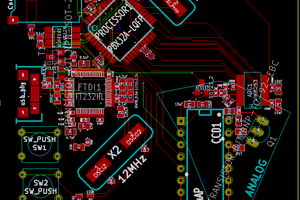
any update on the c00l CT prototype?

  Are you sure? yes | no

Ahron Wayne wrote 08/18/2023 at 00:05 point

Loved your last few posts! But I'd love to have seen your second and 3rd, with much longer integration times! Could have had years worth by now --- though I suppose the barium has a half love of about 10.. 

  Are you sure? yes | no

peter jansen wrote 08/20/2023 at 17:30 point

thanks!  It would definitely have been cool to have just left it running for weeks (or months) to empirically see the kind of reconstruction resolution you could get with this very low-intensity source -- though I calculated it out, and it was still of course quite low (it'd probably take weeks for a modest reconstruction of a bell pepper).  My wife became pregnant with our little one shortly after I built this, so I of course stopped all my radioactive science, and never ended up running those long integration time experiments.  

  Are you sure? yes | no

Ahron Wayne wrote 08/21/2023 at 00:36 point

 Yeah, it would have been cool to see a super long reconstruction. I was thinking of trying with an americium source which has even fewer and softer actual x-rays emitted, with an older flat panel detector. But then I got my actual x-ray source working and it makes things a bit easier! Congrats on having a several year old human now!

  Are you sure? yes | no

Marcin Wachowiak wrote 07/26/2018 at 19:49 point

Hello, could you please tell me the estimated lenght of the pulse that is generated by the photodiode? Is it like 300ns or a few us? I was wondering if an additional peak detector would be required for the circuitry in a quite similar radiation detector.

  Are you sure? yes | no

peter jansen wrote 07/26/2018 at 20:08 point

Hi Marcin, I saw the beginnings of your detector project the other day -- I think it's great, and I'm eager to see what you come up with!  A lot of the details on the detectors in the OpenCT2 are available in the earlier posts -- this post ( https://hackaday.io/project/5946/log/18818-improving-the-parallel-detector-with-photodiode-stacking ) and earlier ones show scope traces of particle detections, and while the pulse length depends a bit on energy level (since it takes time to decay back to baseline), I think it's generally between 3-10uSec. You can definitely add a peak detector circuit to keep the pulse at maximum height, read off the height with an  ADC, and then reset it -- but for significant count rates (i.e. near a source, rather than just background) the process does have to be pretty fast -- detection events end up stacking ontop of each other, and the waveform gets a bit messy.   I think I worked to design something similar a few years ago that worked as a backpack that would sit on the Radiation Watch Type 5 detector, the indent being to use it for spectroscopy by reading the energy levels.  I never quite got it to work, and some additional reading (I'm not a particle physicist) suggested that those doing spectroscopy tended to have to place in some pulse shaping circuitry to make the peak meaningful -- and then I got busy and didn't continue.  I'm happy to try and dig up the most recent design I had with the understanding that it's probably not complete, incase it's helpful to you. 

  Are you sure? yes | no

Marcin Wachowiak wrote 07/26/2018 at 20:17 point

Thank you very much for that lot information, it's quite promisig that those pulses are pretty long. I could analyse them with STM32 ADC, but I already designed a peak detector using OPA615 and now I'm starting to doubt it's utility... will see.

  Are you sure? yes | no

peter jansen wrote 07/27/2018 at 19:37 point

It's a deceptively challenging problem, and doing a bunch of reading (or, better, finding someone who has designed a PIN-photodiode based spectroscopy detector and who understands the pulse shaping issues) would be a great start -- and if you could pool these resources together for the rest of us, that would be great, too.  

It looks like I already published a recent version of the peak detector -- it's quite simple, and available here, in case it helps your project: https://github.com/opensensinglab/radiationwatchbackpack .  I've at different points tried adding microcontrollers onto the board with the detection circuitry, but it usually ends up adding so much noise as to be unusable.  They really are remarkably sensitive circuits, but when you think that they're literally detecting single photons, it puts things into context. :)

  Are you sure? yes | no

Marcin Wachowiak wrote 02/21/2019 at 17:13 point

After digging deep into the topic and searching the web I found a scientific publication concerning X-ray imaging using BPW34 ( available here: https://kundoc.com/pdf-a-low-cost-x-ray-imaging-device-based-on-bpw-34-si-pin-photodiode-.html ) In this case they obtained quite nice images at the cost of irradiating the object with rays from dental tube. The thing that surprises me the most, is the use of unintegrated operational amplifier made from discrete components. I’ll just leave it here for anyone interested.

  Are you sure? yes | no

V.Z. wrote 12/12/2017 at 20:06 point

Peter, excellent project! I'd really like to replicate your system. The problem is, I can't find a source for radioisotopes where I'm temporarily based (UK).
If anyone here are based in UK - do you know where/if one can obtain radioactive source without a license/for personal use? Best I could find was that schools can buy a limited range http://practicalphysics.org/radioactive-sources-isotopes-and-availability.html

  Are you sure? yes | no

Brian wrote 06/05/2016 at 16:38 point

Hello, Have you looked into liquid ionization chambers for detection? They would give you increased interaction volume with the X-rays. They are being used in arrays for imaging more and more. I have yet to see one home built, but it may give you higher count rates for faster scans. Here is an example- 

http://www.ptw.de/liquid-filled_ion_chambers.html

  Are you sure? yes | no

John wrote 04/03/2016 at 19:01 point

Hi Peter, 

I was wondering if you could use the burr brown OPT210 (integrated photodiode + opamp) as a detector. If I compare the specs with the circuit requirements of maxim AP2236 it seems to fullfil the requirements. And it would greatly improve the density of detectors you can use.

Another question: are you detector boards for the BPW34 + amplifiers available for purchase?

Thanks! 

  Are you sure? yes | no

peter jansen wrote 04/05/2016 at 06:45 point

Hi John,

That is an interesting part -- but it looks like it's passed it's end of life, and I can't seem to easily find the replacement for it.  The specifications on the photodiode look like it has a very high capacitance (~500pF), which might make it too high to work well for this task -- but then, the best way is simply to run an experiment and try.  I think one of the reasons that the BPW34 tends to be popular for this task is that out of an assortment of photodiodes that folks have used in this past decade for low-cost detection, for whatever reason the BPW34 just happens to (likely accidentally) have very good performance, especially for the price point. 

I'd love to do a small run of the detector boards if there's interest, once the OpenCT2 design is reasonably complete and the detectors are very well characterized, so folks know what they're getting into.  Given that the TI instrumentation amplifier is very pricey, this will likely involve a bit of experimentation to see if a less expensive part can be substituted while still maintaining most of the performance.  If you're looking for a very small radiation sensor without needing it for imaging, the Type 5 detector from Radiation Watch is very good (and is what I used in the first OpenCT), and has a larger photodiode area, so it's much more suited to detection than imaging.  With the opamp backpack from the original OpenCT project, it's also possible to make the Type 5 much more sensitive by calibrating the detection threshold to be just above the noise floor.  The same procedure is used for the detectors here in the OpenCT2, only automatically using the digipot. 

  Are you sure? yes | no

John wrote 04/05/2016 at 20:22 point

Dear Peter,

Indeed, I was not aware that OPT201 was no longer in production. TI's website still has the OPT101 and OPT301. Further I saw the IVC102, a "Precision Switched Integrator Transimpedance Amplifier", basically it is a OpAmp integrator with a reset switch. Not sure if the charge generated by your high energy photons is enough for detection by IVC102, but could be an alternative to think about. I will drop a message if I manage to source them for a good price.

  Are you sure? yes | no

Ryan Shill wrote 02/19/2016 at 14:10 point

Sand the lasered panels!

  Are you sure? yes | no

Richard Jennelle wrote 02/18/2016 at 20:26 point

I see sources available with decent kV output that are clocking 100 uCi. Why not use Co 57?

http://www.imagesco.com/geiger/radioactive-sources.html#sources

Way cool idea,

Rick

  Are you sure? yes | no

peter jansen wrote 02/18/2016 at 21:56 point

Most of Cobalt 57's emissions are well above 100keV, which means they're of such high energy that they sail through most materials (making them not terribly good for absorption images of some things, like organic matter).  Their high energy also means they're much less efficiently detected directly by a silicon PIN photodiode, and would need a different setup, like a scintillator, incorporated into the detectors.   From memory, I think most x-ray tubes for CT scanners tend to emit in the ~60keV range.  The detectors on this device are theoretically most efficient around 10keV, but the noise floor is probably closer to 30-40keV, so emissions lower than that would be (unfortunately) challenging to detect.   Thanks for the question!

  Are you sure? yes | no

AssidiousBlue wrote 01/11/2016 at 10:56 point

Hi Peter,

Hope all comes along. Congratulations on the Prof Place, may tenure come eventually. Sorry I never thanked you for your response below; for some reason I missed it every time I looked.

One last little idea. I believe that you can oppose photodiodes, such that one stack will cause a positive current from your, and the other a negative one. That is, one stack has it's cathode to the input, and the other has an anode to the opamp input. The downside is the requirement for an even higher voltage for the second stack, and that would push it past extreme low voltage (<50-60VDC in most jurisdictions).

It might be a relatively simple trick to either double the active surface area, or increase the sensitivity to particles within that area, with minimal additional circuitry (same opamp, same ADC).

Two downsides come to mind; the aforementioned additional bias current (bias*2), and the potential for simultaneous detections cancelling each other (although you already have the issue of simultaneous detections because of stacking the PINs).

My last A$0.02 regarding noise issues and the detector cards; would chucking an additional 10nF capacitor in the input bias and 5v lines (you could simply stack them to test) help with ripple, can you increase the frequency on your switching sources so they are higher than your nyquist limit, or lower them to within the nyquist limit (I forget which might help), and would increasing the isolation between your 5v and Bias, as well as ground-fencing the PIN bias / opamp seperate from the rest of the ground plane help (and does it need two ground planes.

Keep up the good work, and don't neglect the OMRI forever please :)

As always, I'm clinical not engineering, all knowledge is outside my field but within my interests.

EditL This is an intriguing TI application note regarding power supplies; http://www.ti.com/lit/an/sbaa203/sbaa203.pdf ; 4 of these REF5010 packages gives you you a nice 3-8ppm 40v line as they can act like an ideal Zener diode (supposedly), you can also use the REF5050 for your Opamps?

  Are you sure? yes | no

Andrew Starr wrote 12/08/2015 at 08:19 point

Hi Peter,

Here's a whimsical idea: according to wikipedia, the radioactivity of brazil nuts is about 1-7nCi/g. So if you got together, say, 10kg of brazil nuts, that would give you a radiation source about 5x greater than your Ba-133 source (assuming ~5nCi/g average). 

So how much are brazil nuts where you are? :)

  Are you sure? yes | no

peter jansen wrote 12/08/2015 at 23:32 point

Hi Andrew,

For imaging, you'd need a point source (or something with a relatively small area of emissivity), so having a giant bag of brazil nuts wouldn't work very well.  But it's certainly a hilarious mental picture!

In general, the radioactivity limit is I think a good one -- there are certainly sources that one could find that are more intense with the proper licensing and precautions, but I think that's out of the scope of this project, which aims for using extremely low intensity sources to ensure a low level of risk.  With the signal dominated by shot noise, I'd be more interested in a (still ultra-low intensity) source with a more predictable emission pattern, though with my knowledge of high-energy particle generation, I'm not sure what that would look like.  There's plenty of absorption imaging that can be done with a baseline of only 70 counts if you know there will be very close to 70 counts each minute, but if that rate varies from 40 to 100, you end up needing to integrate much longer to reduce the variance and get a more accurate average estimate of absorption (at the expense of a much larger dose).

  Are you sure? yes | no

Andrew Starr wrote 12/09/2015 at 08:24 point

Heh. A big box of brazil nuts with a lead pipe collimator? :)

  Are you sure? yes | no

Chrismck wrote 08/16/2015 at 14:42 point

Peter, On your detector boards - have you considered using Black Plasti-dip rather than the electrical tape? Would save substantial time wrapping boards.   I personally have not checked it to see if it is conductive but I would think it isn't once dried.  This would allow you to 'dip' the board (use the paint can not the spray version) up to the point you want to mask from light/or electrically.  It's also very easy to remove by peeling the product off.  I have a can sitting waiting for the next project that has such a need.

By the way absolutely love this project... great attention to detail, awesome the way it's progressing.

  Are you sure? yes | no

peter jansen wrote 08/16/2015 at 19:49 point

That's a really clever idea!  I've based the wrapping procedure to approximate what I think is happening with the Radiation Watch Type 5, but I've always wondered what that would look like on an assembly floor -- possibly having to have a human manually do the wrapping, and incurring the assembly expenses associated with this.  It's possible that your plasti-dip idea might be a great time saving alternative!  Thanks! 

The new microcontroller board arrived this weekend, and I've just assembled it -- hopefully within a few weeks we'll be able to see the first low-resolution data!

  Are you sure? yes | no

jul wrote 06/02/2015 at 17:18 point

Plastic scintillators exixts for the whole spectrum : alfa, rontgen, beta, gamma and neutrons.  The cost is less then a BGO.

  Are you sure? yes | no

jul wrote 05/30/2015 at 23:09 point

why not using a scintilator plastic followed by a foton detector, this gives a higher yield in fotons

  Are you sure? yes | no

peter jansen wrote 06/02/2015 at 07:16 point

It's a good question.  I think scintillation crystals are often used for higher energies, where the detection efficiency using a bare silicon PIN photodiode (without a scintillatior) is dominated by compton scattering, and very inefficient.  For the low energies of Ba133 (~30-35keV), I think it might still be on the edge of the photoelectric effect, and somewhat more efficient at this.  I had originally tried Cd109 since it's emissions are ~20keV and should be much more efficiently detected, but unfortunately it's well under the noise floor (and Cd109 has a relatively short halflife).  I have a chunk of BC-408 as well as some BGO crystals from a decommissioned CT scanner, but even if these worked well for such low energies and had a matched photodiode for their emission spectrum, this would increase the cost of each detector by at least an order of magnitude (and they'd likely be much bigger).  I'd certainly be curious to know what one might expect in terms of counts with an appropriate scintillator, though, if someone with a bunch of scinatillator experience happens to see this!

  Are you sure? yes | no

AssidiousBlue wrote 05/30/2015 at 22:16 point
May I suggest multiple rows of sensors in addition to multiple sensors? Or potentially, one larger, crescent-shaped board pre row with many sensors on the single board, and then the boards could be stackable so that you have a matrix-array. Would a copper shield give you slightly better attenuation of noise? Are you thinking of using coded apeture? Or is the detection frequency too low? What is the decay time of a detection on the pin-diode, and is the opamp used fast enough in it's slew rate, frequency response? And finally, I know you don't want to use higher-curie sources, but have you considered stacking disks and then collimating them? @Simon, I think the detection frequency is too low, brief and uncontrolled to make increased SNR with attenuation of both Clinician, not technician, so just asking/offering uninformed suggestions

  Are you sure? yes | no

peter jansen wrote 06/02/2015 at 06:33 point

Thanks for your suggestions.  I'll try to organize a bit, since you bring up a lot of points!

(1) Multiple rows of sensors are technically possible, but since you'd be making projections at off-angles and through more material, they wouldn't be ideal -- you'd still have to make lots of measurements to back out the volumetric data.  It would also be physically challenging to fit the amplifier circuit on such a densely packed array. 

(2) Single large crescent-shaped detector: I had considered this initially, but the density would simply be too high, so I went with the modular approach.  It's also a lot easier to make many inexpensive single-sided modular detectors, and it's more amenable to open source design -- someone can reuse it for their project, using only one or several detectors. 

  Are you sure? yes | no

peter jansen wrote 06/02/2015 at 06:40 point

(3) Coded-aperture:  It'd certainly be interesting to try a coded aperture approach, but I'm not sure how you'd manufacture a small x-ray lens -- and even if you could, it's not likely that others would be able to repeat it.  It also would be somewhat technically challenging to make the code strip (out of quite thick lead, but with fine enough detail to resolve the sample spatially), and to physically translate it.  

(4) Stacking sources is strictly out and not legal -- I'd like to keep this quite safe, and not have to worry about licensing, or regulatory issues.  

  Are you sure? yes | no

Simon wrote 05/30/2015 at 07:10 point

Have you looked at using phase sensitive detection to improve your snr? This is used quite a lot in low signal level optics experiments.

  Are you sure? yes | no

peter jansen wrote 06/02/2015 at 06:25 point

Hi Simon, thanks for your suggestion.  I think one of the requirements of using a phase-lock amplifier is having a continuous signal, or at least an approximately-continuous signal on the timescale of your signal.  Since here each detection is a discrete event that occurs very infrequently (about once per second, for 1uSec, or about one millionth of the time), that violates the continuity assumption.  Even if the signal was approximately continuous on the ~kHz to mHz rates that you might have to modulate the signal at, I'm not sure how you'd physically go about that, other can making a giant chopper wheel out of lead... and that would not be small or easy to move. :)

  Are you sure? yes | no

Similar Projects

Does this project spark your interest?

Become a member to follow this project and never miss any updates