-
Changing I2C Clock Speed [SDC] on Banana Pi BPI-M2 ZERO (Armbian)
03/15/2023 at 01:13 • 0 commentsAfter much searching for how to change the I2C clock speed [SDC] on Banana Pi BPI-M2 ZERO running Armbian, with a little experimentation I found a way to alter the device tree (DT) parameters to accomplish the task.
I've not tried other SDC clock frequencies besides 100kHz and 400kHz, so let me know if other (higher or lower) speeds work for you - your "mileage may vary".
This approach may also work for other platforms running Armbian, however you'll have to locate the design tree file for your specific platform - and there are many in the installation I'm using.
It's assumed that you have already turned on I2C0 using the "armbian-config" utility.
Your user account will need root (sudo) privileges to perform these steps:- Locate the design tree file for the BPI-M2-Zero platform - typically in the /boot/dtb directory.
cd /boot/dtb
ls -l *m2-zero*

-rw-r--r-- 1 root root 34592 Mar 12 20:11 sun8i-h2-plus-bananapi-m2-zero.dtb
There are two formats of the device tree file. DTB --> binary format. DTS --> source (plaintext) format. We'll want to convert the m2-zero's DTB file to plain text (DTS) so it can be edited.
First, create a backup of the DTB file just in case things go horribly wrong.
sudo cp sun8i-h2-plus-bananapi-m2-zero.dtb sun8i-h2-plus-bananapi-m2-zero.dtb.bak
Next, make a DTS (editable) file from the binary. This is done using the dtc (Device Tree Compiler) utility. You can get help by entering "dtc --help" or consulting the manpages by entering "man dtc".
sudo dtc -I dtb -O dts -o sun8i-h2-plus-bananapi-m2-zero.dts ./sun8i-h2-plus-bananapi-m2-zero.dtb
Load up your freshly created dts file. I'm using emacs, however you can use your favorite editor. Nano will work as well.
sudo emacs sun8i-h2-plus-bananapi-m2-zero.dtsSearch for the section that controls the I2C0 configuration. In this case I2C0 is the one at address 1c2ac00. How do I know that? By having searched further in the DTS file being edited for "i2c0" and finding the corresponding address reference. For BPI-M2-Zero in this case:
i2c0 = "/soc/i2c@1c2ac00";![]()
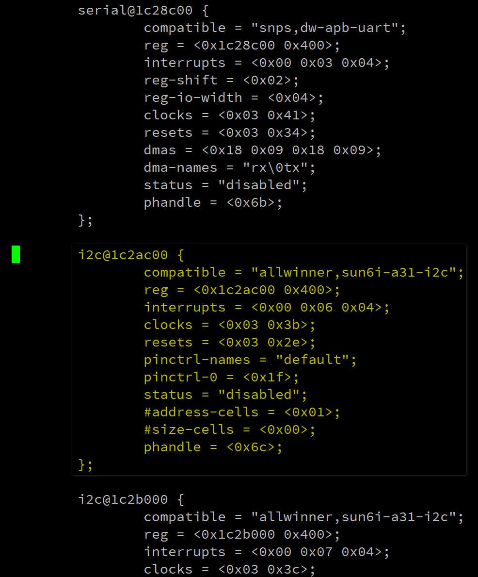
If it doesn't already exist in the I2C0 control block, insert the clock-frequency parameter...
clock-frequency = <400000>;... so that it looks like the screenshot below. So far, I've tried both 100000kHz and 400000kHz and validated the resulting SDC frequencies using a multi-channel logic analyzer.
![]()
At this point, save the file and exit the editor.
Lastly convert the edited DTS file back to DTB format
sudo dtc -I dts -O dtb -o sun8i-h2-plus-bananapi-m2-zero.dtb ./sun8i-h2-plus-bananapi-m2-zero.dtsFinally - reboot for the changes to take effect.
sudo reboot
Please let me know if this solution works for you. I'm open to being educated on other methods as well. I'm especially interested in software control of this parameter - using IOCTL or some other means.
Inspiration and credit where credit is due:
https://forum.armbian.com/topic/15348-orange-pi-3-change-i2c-speed/
https://github.com/armbian/config/issues/111
https://forum.armbian.com/topic/3030-h3-i2c-speed/#comment-21132
- Locate the design tree file for the BPI-M2-Zero platform - typically in the /boot/dtb directory.
-
Alchitry IO Element Graphic Layout
01/09/2021 at 01:59 • 0 comments![]()
-
Alchitry Au - Clock Talk
01/03/2021 at 00:44 • 0 commentsHow to generate alternate clock signals for Xilinx Artix-7 FPGA and Alchitry Au
This article started out by asking a simple question: "What if I wanted to drive my Alchitry Au FPGA design with something other than the 100Mhz master clock? " What resulted was a trip down a rabbit hole that was as distracting as it was rewarding.
If you'd like to be spared the deep-dive and get right to a concrete example, you can skip to the end for a practical introduction and come back here to understand the underpinnings of what's going on.
From the top-level documentation for the Alchitry Au FPGA, featuring the features a Xilinx XC7A35TFTG256, we know the on-board clock is 100MHz and that it can be multiplied internally by the FPGA.
- How is the master clock generated and input into the FPGA?
- How is the FPGA configured to use this particular clock input?
- How is this clock made available to other FPGA resources?
- How can other clocks be synthesized from the master clock and distributed within a design?
This user joined on 05/19/2019.
My Pages
Projects I Like & Follow
LoRa 2.4Ghz module used in full duplex mode, sending/receiving MavLink telemetry data
Share this profile
ShareBits
Become a Hackaday.io Member
Create an account to leave a comment. Already have an account? Log In.


 Slaven Damjanovic
 Alex Klimaj
 Yohan Hadji
 Irene Wolf
 Simon Merrett
 David Prutchi
 Leonardo Miliani
 Steven
 Akio Sato
 Cees Meijer
 Thomas Buck
 John Opsahl
 alnwlsn
 Fabian
 Stefan Wagner
 Max2Play
 Marcelo
 Eric Sims