 Frank Buss
 Debargha Ganguly
-
DIY breadboard push button
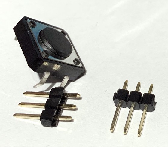
04/26/2019 at 20:50 • 0 commentsMost buttons can't be used with a breadboard because the pins are too short. For example these nice button I bought for $0.12 each. But you need only some pin headers to fix this:
![]()
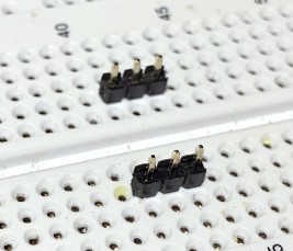
First plug in the pin headers in a breadboard:
![]()
Then clip the button on the pin headers. You might need to bend the pins of the button a bit so that it is a tight fit and the pins of the button are at the outer side of the pin headers on each side, so that it doesn't fall off when you solder it:
![]()
Then solder it, done:
![]()
You can buy a professional PCB for it now in my Tindie shop as well:
https://www.tindie.com/products/frankbuss/breadboard-push-button/
-
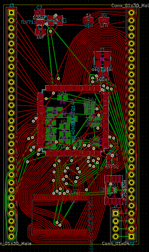
Programming an iCE40HX4K with an Arduino and Python
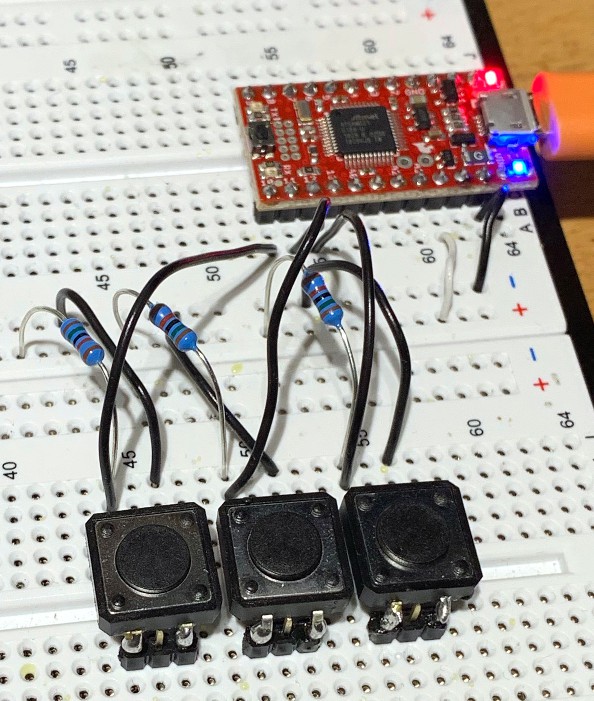
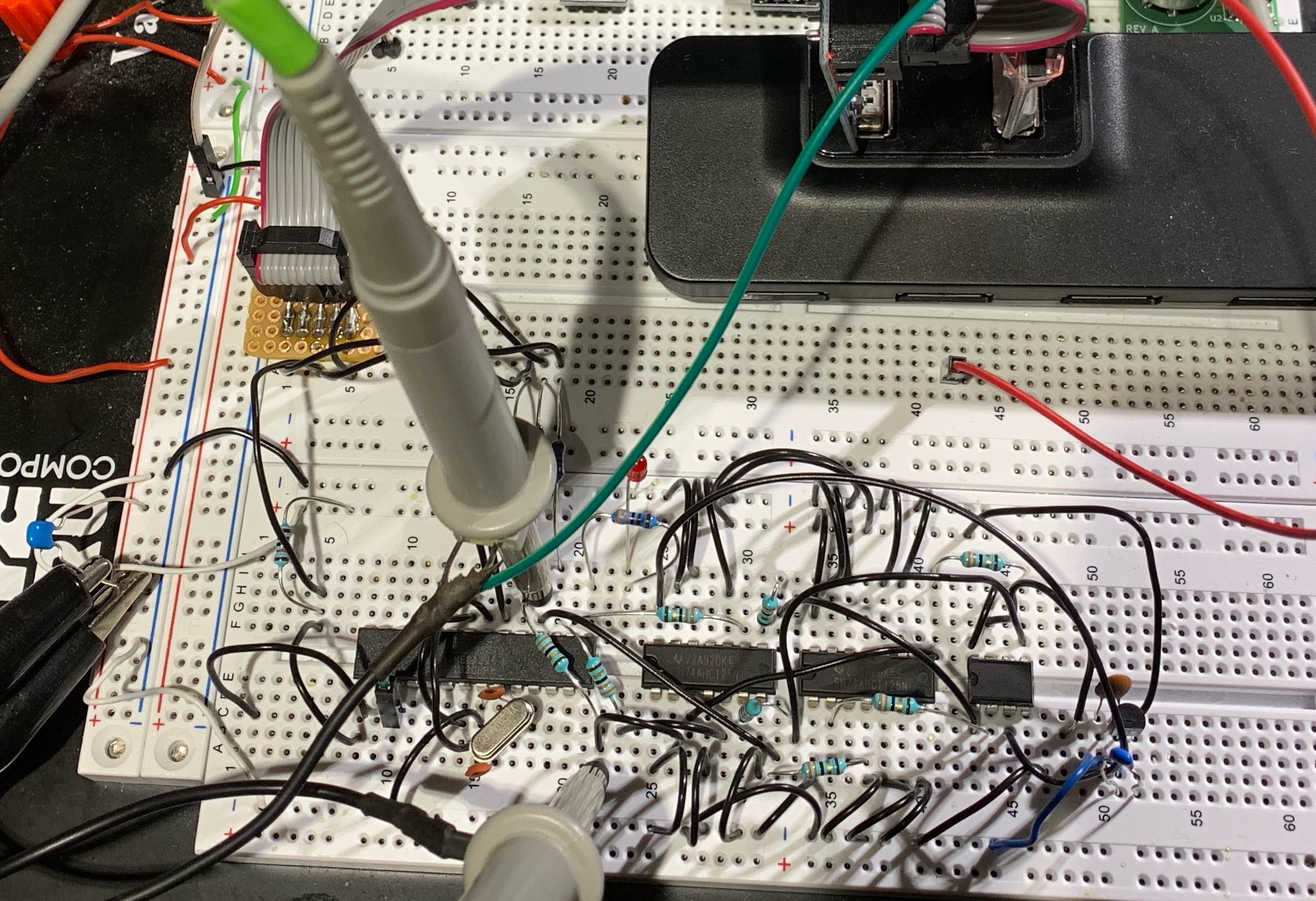
04/19/2019 at 13:05 • 0 commentsYou can program an iCE40 FPGA with a microcontroller, for example an Arduino with 3.3V IO. I tested it with a SparkFun SAMD21 Mini Breakout and a custom board. This is the setup:
![]()
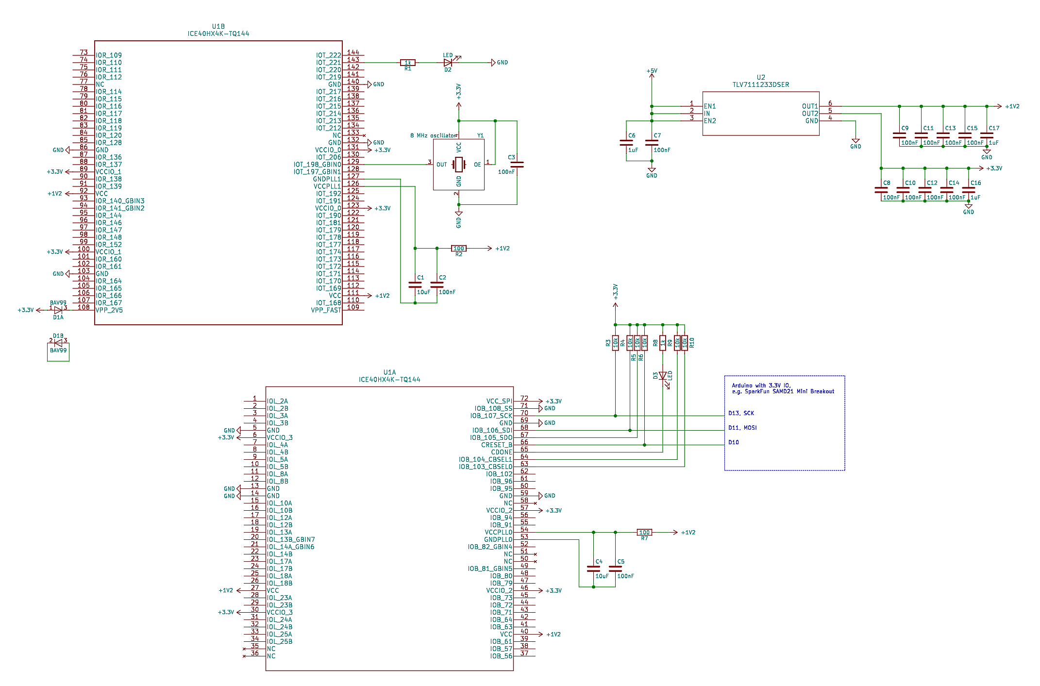
I have an additional flash and SRAM on my board, but you don't need this for a minimal test setup. This is the minimal circuit diagram how to use the FPGA (click on the image to zoom in) :
![]()
The routing was done with TopoR:
![]()
With the iCEcube2 IDE I wrote this test program:
library IEEE;
use IEEE.STD_LOGIC_1164.all;
use IEEE.numeric_std.all;

entity top is
    port (
        clk : in STD_LOGIC;
        led : out STD_LOGIC
    );
end top;

architecture Behavioral of top is
    signal blinker : natural range 0 to 25000000;
    signal blink : std_logic;

begin
    process (clk)
    begin
        if rising_edge(clk) then
            blinker <= blinker + 1;
            if blinker = 4000000 then
                blinker <= 0;
                blink <= not blink;
            end if;
            led <= blink;
        end if;
    end process;
end Behavioral;
When I compile it, I get the file "test_Implmnt/sbt/outputs/bitmap/top_bitmap.bin".
It is easy to configure the FPGA: First set the CRESET_B pin to low to reset the FPGA. Then hold down the SS pin and set CRESET_B to high, which starts the SPI slave configuration mode. You can then send the bin file data with the SDI and SCK pins.
On the Arduino side I wrote this script for the transfer:
#include <SPI.h>

#define RESET_PIN 10

#define ACK 6
#define NAK 21

const int BUF_SIZE = 128;

uint8_t buffer[BUF_SIZE];

void setup() {
  pinMode(RESET_PIN, OUTPUT);
  SerialUSB.begin(115200);

  SPI.begin();
  SPI.beginTransaction(SPISettings(1000000, MSBFIRST, SPI_MODE0));
}

void readBlock() {
  // wait for block start
  unsigned long t0 = millis();
  while (true) {
    if (SerialUSB.available()) {
      break;
    }
    unsigned long t1 = millis();
    if (t1 - t0 > 1000) {
      // timeout
      SerialUSB.write(NAK);
      return;
    }
  }

  // read data
  int received = SerialUSB.readBytes((char*) buffer, BUF_SIZE);
  if (received != BUF_SIZE) {
    // timeout
    SerialUSB.write(NAK);
    return;
  }

  // send with SPI
  SPI.transfer(buffer, BUF_SIZE);

  // acknowledge
  SerialUSB.write(ACK);
}

void loop() {
  // read command
  char cmd;
  while (true) {
    if (SerialUSB.available()) {
      cmd = SerialUSB.read();
      break;
    }
  }

  // execute command
  switch (cmd) {
    case 'r':
      // reset
      digitalWrite(RESET_PIN, LOW);
      delay(10);
      digitalWrite(RESET_PIN, HIGH);
      delay(10);
      SerialUSB.write(ACK);
      break;
    case 'b':
      readBlock();
      break;
    default:
      SerialUSB.write(NAK);
  }
}
And then I could upload the bin file with this Python script:
#!/usr/bin/python3

import serial

ACK = 6
NAK = 21

ser = serial.Serial('/dev/ttyACM0', 115200, timeout=1)

# read and evaluate response
def readResponse():
    d = ser.read(1)
    if len(d) == 0:
        raise Exception('response timeout')
    if d[0] == ACK:
        return
    if d[0] == NAK:
        raise Exception('NAK received')
    raise Exception('unkown response')

# send a command
def sendCommand(cmd):
    ser.write(cmd.encode())
    readResponse()

# send a block
def sendBlock(data):
    ser.write('b'.encode())
    for d in data:
        ser.write([d])
    readResponse()

# read file and add some bytes at the end for the required 49 clocks for configuration
inputFile = open('top_bitmap.bin', 'rb')
bufSize = 128
data = bytearray(inputFile.read()) + bytearray([0] * (bufSize * 2))

# reset FPGA
sendCommand('r')

# send data to FPGA
while len(data) > bufSize:
    block = data[:bufSize]
    data = data[bufSize:]
    sendBlock(block)
At the end of the upload the CDONE pin goes low, if there was no error. I added an LED to it which goes off when it is done.
The other LED on pin 143 blinked with 1 Hz after the configuration, as programmed in the VHDL file.
-
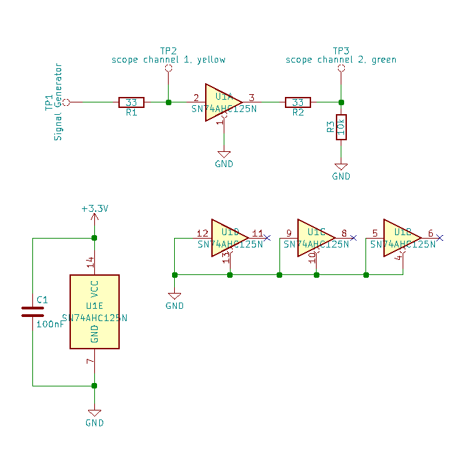
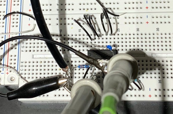
voltage level translators
04/13/2019 at 13:11 • 0 comments5 V to 3.3 V
Test circuit with a SN74AHC125N, bought here, for the 5 V to 3.3 V level translation:
![]()
Signal generator: Siglent SDG1050, 50 MHz max output frequency
Oscilloscope: Agilent DSO-X 3012A, 100 MHz analog bandwith, 4 GSa/s samplerate
Test setup:
![]()
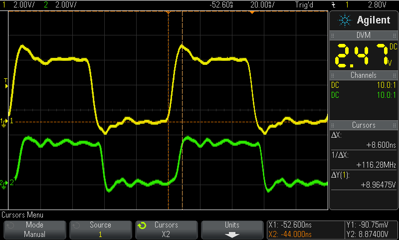
Result for 10 MHz:
![]()
Less than 10 ns propagation delay, fast edges.
3.3 V to 5 V
Result for a SN74AHCT125N, bought here, same circuit and test setup, but with 5 V supply for the buffer and 3.3 V for the signal generator, to test the 3.3 V to 5 V level translation:
![]()
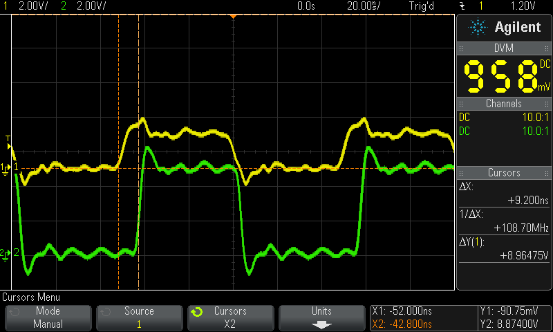
A little bit slower, but still less than 10 ns propagation time and fast edges. The datasheet guarantees high level signal detection down to 3 V, but it works even with 2 V:
![]()
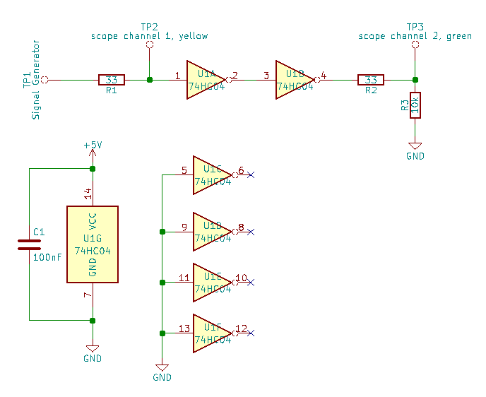
Test with a CD74HC04E hex inverter
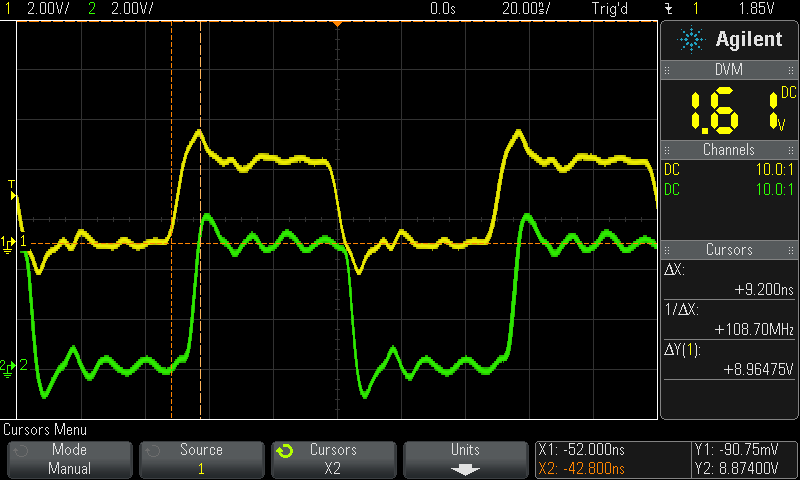
Test circuit with a CD74HC04E, bought here:
![]()
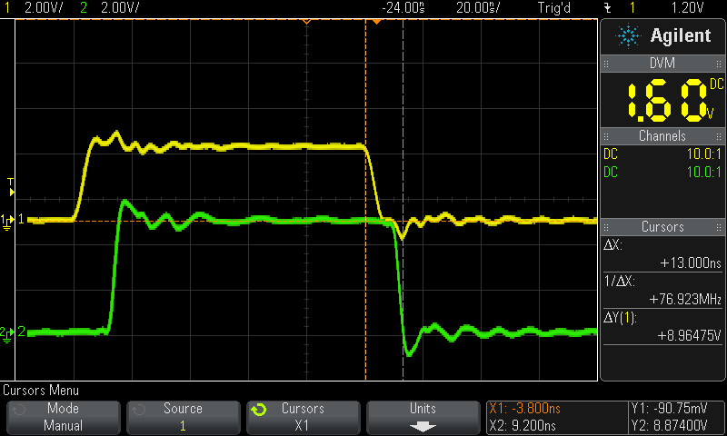
Doesn't work with 2 V for the input signal and gate propagation time is longer than 10 ns. With 3.3 V at the input and 5 V for the supply it looks like this:
![]()
Fully working example with FRAM
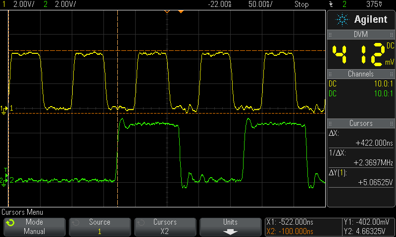
This is an example with the SN74AHC125N and SN74AHCT125N, and an ATmega328 and a FRAM chip. The ATmega328 is running a 5 V, and the memory with SPI port at 3.3 V. Test setup:
![]()
The SPI bus is running at the max possible frequency of 10 MHz. Yellow is the clock signal from the microcontroller and green the MISO signal from the memory, measured at the microcontroller input:
![]()
The combined delay of the memory IC and the gate delays of the voltage translators is less than 20 ns, good enough that the microcontroller can cleanly sample the MISO signal at rising clock edge.
My Pages


Projects I Like & Follow
 timonsku
 Carl Bugeja
 Jdaie
Jdaie Onchip
 deʃhipu
 Jens Hauke
 Scott Swaaley
 SHAOS
SHAOS Aleksandar Bradic
 Fabien-Chouteau
 Jarrett
 Morning.Star
 davedarko
 MorriganR
 Antti Lukats
Share this profile
ShareBits
I'll probe the signals, but both of my units are US versions
I'll probe the signals, but both of my units are US versions
Hey Frank! Thanks for the tips on the vectrex rom. I tried making a couple including biltz, confirmed that it programmed, but it goes to mindstorm as if there is no rom. Any tips? I used a larger cap but it shouldn't make a difference.

Do you have a non-buzz European Vectrex version? Then it doesn't have the NCART signal. You can instead wire the CE signal.
It looks like there are more differences between your Vectrex and US versions. I have 2 units and using the CE signal instead of VCART with no success. I am getting 3.9V where the VCART signal is supposed to be so it is connected to something. And I am reading 3V on the OE line as well so it is not which doesn't look right.
You can't measure it with a multimeter, it is switching fast between 5V and 0V if there ar signals, and the multimeter will show only average values. You would need an oscilloscope. But if there is a VCART signal, my original cartridge should work, at least it does work when I tested it. There are no other differences to my knowledge.
Maybe something went wrong with the EPROM burning? Can you post a link to the file you burned? Did you tried to read it back if it was burned correctly? What EPROM type did you use?
Hey Frank, thanks for following me. Sorry it took me a while to notice, I've not been paying much attention to the feed lately. All been a bit much...
But I'm feeling a lot better, and catching up on weeks of stuff... ;-)
Take care dude :-)