Close
0%
0%

YGREC8

A byte-wide stripped-down version of the YGREC16 architecture

Similar projects worth following
YGREC can stand for many things, such as "YG's Relay Electric Computer", "Yann's Germanium and Relay Equipped Computers" or "YG's Ridiculous Electronic Contraption". You decide !

#YGREC16 is getting pretty large and moving away from the original #AMBAP inspiration, making it less likely to be implemented within my lifetime. So here is a "back to minimalism" version with
* 256 bytes of Data RAM (plus parity ?)
* 8 registers, 8 bits each (including PC)
* fewer relays/gates than the YGREC16
This core is so simple that I focus now on other issues, such as the debug/test access port, the register set's structure, I/O, power reduction...
Like the others, it's suitable for implementation with relays, transistors, SSI TTL, FPGA, ASIC, you name it (as long it uses boolean logic)!

After the explorations with #YGREC-РЭС15-bis, I reached several limits and I decided to scale it down as much as possible. And this one will be implemented both with relays and VHDL, since the YGREC8 is a great replacement for Microchip's PICs.

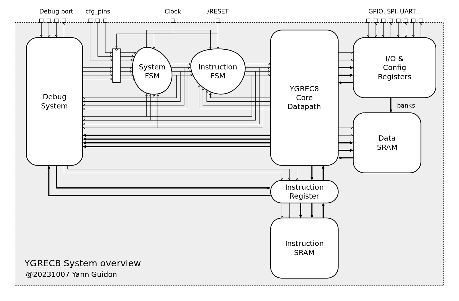
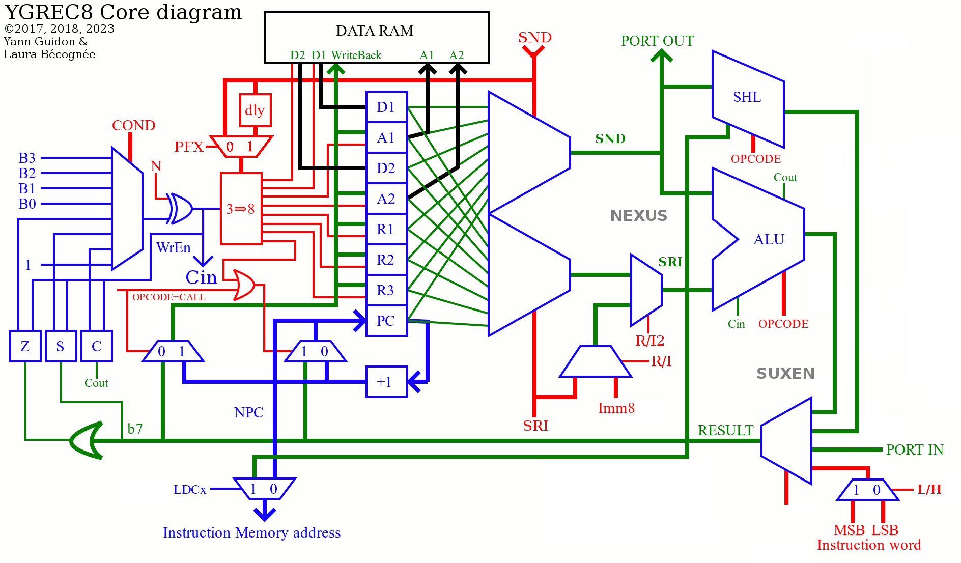
A significant reduction of the register set's size is required so I/O must be managed differently, through specific instructions. The register map is now:

  • D1  <= for NOP
  • A1
  • D2
  • A2
  • R1
  • R2
  • R3
  • PC  <= for INV

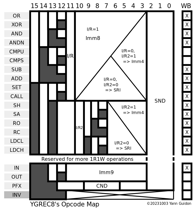
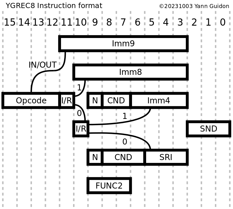
The instruction word is shrunk down to 16 bits. It is still reminiscent of the YGREC16 older brother but I had to make clear cuts... The YGREC8 is a 1R1W machine (like x86) instead of the RISCy YGREC16, to remove one field. Speed should be decent, with a pretty short critical datapath, and all the instructions execute in one clock cycle (except the LDCx instructions and computed writes to PC).

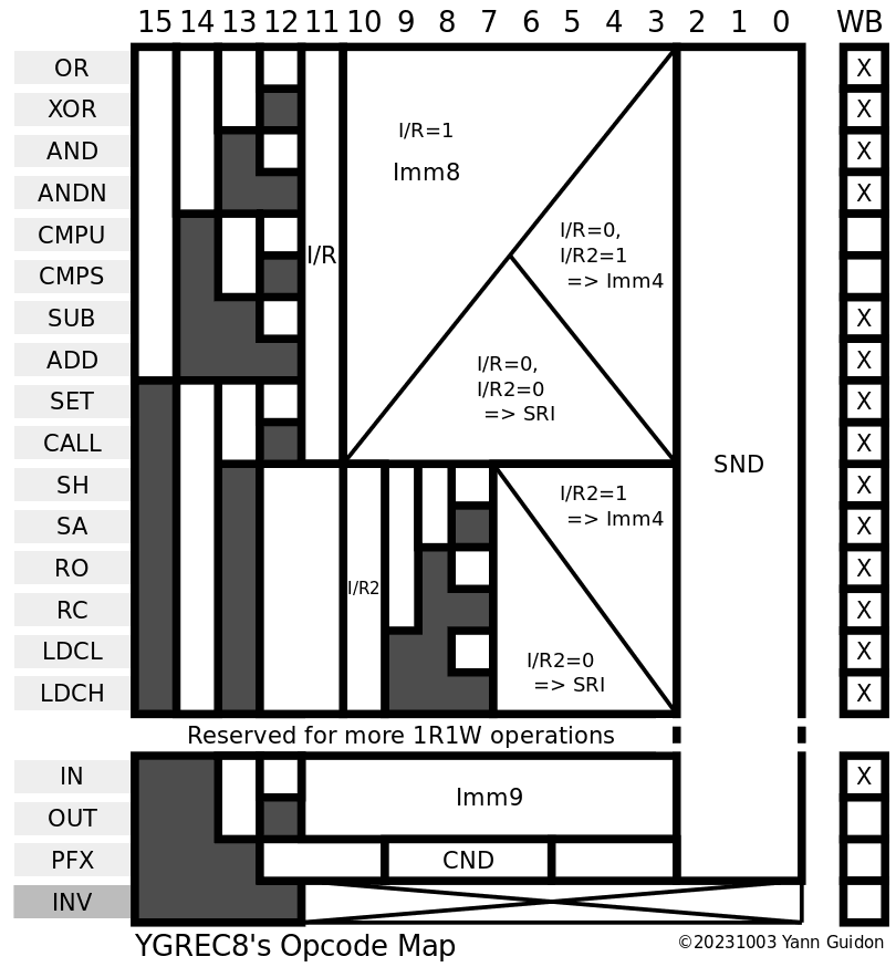
The fields have evolved with time (I have tried various locations and sizes). For example:

20171116: The latest evolution of the instruction format has added a 9-bits immediate field address for the I/O instructions.
20180112: Imm9 is now removed again...
20181024: changed the names of some fields
20181101: modified the conditions to change Imm3 into Imm4
20180112: Imm9 back again ! (for speed/latency reasons, no register operand is provided, an indirect IO register is used instead, and having more IO space is more desirable, otherwise only imm4 is available if a register operand is used)

There are 18 useful opcodes (as many as EDSAC plus INV, and the pseudo-opcodes HLT and NOP), and most share two instruction forms : either an IMM8 field, or a source & condition field. The source field can be a register or a short immediate field (4 bits only but essential for conditional short jumps or increments/decrements).

The main opcode field has 4 bits and the following values:

Logic group :

  • OR
  • XOR
  • AND
  • ANDN

Arithmetic group:

  • CMPU
  • CMPS
  • SUB
  • ADD

Deprecated:

Beware : There is no point to ADD 0, so ADD with short immediate (Imm4) will skip the value 0 and the range is now from -8 to -1 and +1 to +8. (see 17. Basic assembly programming idioms)

Shift group (optional)

  • SH/SA direction is sign of shift, I/R(bit9) is Logic/Arithmetic flag.
  • RO/RC direction is sign of shift, I/R(bit 9) allows carry to be rotated.

Control group:

The COND field has 3 bits (for Imm4) or 4 bits, more than YGREC16, so we can add more direct binary input signals. CALL is moved to the opcodes so one more code is available. All conditions can be negated so we have :

  • Always
  • C (Carry)
  • S (Sign, MSB)
  • Z (Zero, all bits cleared)
  • B0, B1, B2, B3 (for register-register form, we can select 4 bits to test from user-defined sources)

(notice the mnemotechnic trick: ACSZ are in alphabetical order)

Instruction code 0000h should map to NOP, and the NEVER condition, hence ALWAYS is coded as 1.

Instruction code FFFFh should map to INV, which traps or reboots the CPU (through the overlay mechanism): condition is implicitly ALWAYS because it's a IMM8 format.

Overall, it's still orthogonal and very simple to decode, despite the added complexity of dealing with 1R1W code.


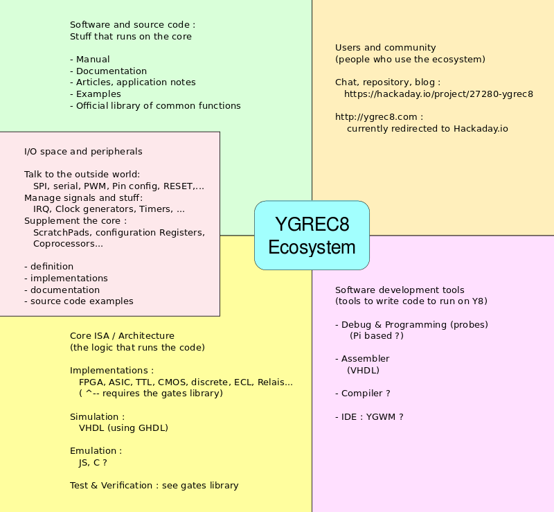
This project is more than an ISA or one implementation : the goal is to become a platform. See log 82. Project organisation

Logs:
1. Honey, I forgot the MOV
2. Small progress
3. Breakpoints !
4. The YGREC debug system
5. YGREC in VHDL, ALU redesign
6. ALU in VHDL, day 2
7. Programming the YGREC8
8. And a shifter, and a register set...
9. I/O registers
10. Timer(s)
11. Structure update
12. Instruction cycle counter
13. First synthesis
14. Coloration syntaxique pour Nano
15. Assembly language and syntax
16. Inspect and control the core
17. Basic assembly programming idioms
18. Constant tables in program space
19. Trap/Interrupt vector table
20. Automated upload...

Read more »

YGREC8_20231012.tbz

The new wave of manuals. No source code yet.

x-bzip-compressed-tar - 141.32 kB - 10/12/2023 at 05:52

Download

x-compressed-tar - 372.71 kB - 11/20/2021 at 14:46

Download

x-compressed-tar - 372.09 kB - 11/20/2021 at 08:56

Download

YGREC8_VHDL.20211118.tgz

assembler refactored, supports DW and re-assembly

x-compressed-tar - 360.31 kB - 11/18/2021 at 17:29

Download

YGREC8_VHDL.20211114.tgz

ALU8 still bork and assembler is incomplete

x-compressed-tar - 359.56 kB - 11/14/2021 at 08:08

Download

View all 59 files

  • Opcode space statistics

    Yann Guidon / YGDES11/20/2023 at 17:53 0 comments

    The new VHDL disassembler is here !

    And the dumb testbench is a great opportunity to collect numbers and figures.

    [ASM]$ grep '[;]' all_opcodes.log |wc -l
    11008
    [ASM]$ grep 'INV' all_opcodes.log |wc -l
    14720
    

    This means that among the 65536 possible instructions, 22% may be re-attributed later, but more importantly, this disassembler provides a clearer picture of how the decoder will work later to detect invalid opcodes.

    The INV opcode only accounts for 4096 instances, and the reserved opcode 1011 has 4096 more. That's 8192 so far. Oh and there are unused opcodes in the 1010 range.

    The above count also includes all the undefined PF fields, as well as some unused bits in the extended opcode range. All those "holes" in the opcode map are flagged with a comment so they can be conveniently tallied.
    ...

    I have also seen that the CALL imm4 instructions look quite dumb but you never know, some "negative addresses" might be trampolines for functions later, and these short forms allow conditional execution. This proves that "going with the architecture", instead of following the quantitative approach of Patterson & Hennessy, can give rise to new coding patterns, structures and interesting techniques.

    Vive l'orthogonalité !

    ......

    And there is more redundancy :

    The assembler checks the immediate value first and if it fits in Imm4 (when applicable), promotes the instruction to Imm4cnd (for the 10 core opcodes). This means to for 10 opcodes, the range -8 to +7 of the Imm8 form is not used. This means 16*10 = 160 unused opcodes.

    ........

    Update !

    The new assembler forces Imm4 to be signed, but the disassembler generates a positive value so only values 0 to 7 are aliased between Imm4 and Imm8, 80 redundant opcodes only (though it still is 160 if the disassembler did output signed numbers and the program counts 640).

    The opcode scan identifies 15743 exceptions to the bijection rule. This includes redundancies, reserved opcodes and unaffected bits.

            diff := instruction_word xor instruction_assembled;
            if diff/="0000000000000000" then
              if
               not (diff ="0000111000000000" and i<38976) and --imm4-imm8 confusion for SRI=0..7
               not (diff ="0000000001000000" and instruction_word(15 downto 12)="1010") and -- reserved bit>
               not (i >= 41728 and i <= 41983) and -- reserved extended opcodes, RR
               not (i >= 42752 and i <= 45055) and -- reserved extended opcodes, IR and unused IR bits
               not (instruction_word(15 downto 12)="1011") and -- RSVD opcode
               not (instruction_word(15 downto 12)="1110" and     -- PF opcode
                    instruction_word(11 downto 10)                  -- IR, IR2
                  & instruction_word( 5 downto 3)/="00000") and     -- SRI
               not (instruction_word(15 downto 12)="1111")   -- reserved opcode
              then
                output_message(SLV_to_bin(diff) & "_");
                mismatch := mismatch+1;
              else
                exceptions := exceptions+1;
              end if;
            end if;
    

    .....

    The new scanner contains some logic that skips the invalid opcodes, which also doubles as a definition of invalid instructions for later.

        OPCODE=Op_RSVD
    or  OPCODE=Op_INV
    or (OPCODE=Op_PF and   -- PF opcode with IR or IR2 or SRI not cleared
          instruction_word(11 downto 10) & instruction_word( 5 downto 3) /= "00000")
    or (OPCODE=Op_EXT1 and
         (( instruction_word(11)='1' or instruction_word(9 downto 8)="11" )   -- 10 EXT1 reserved opcodes
      or  ( instruction_word(10)='0' and instruction_word(6)='1'))) -- unused bit when SRI
    

    The other exceptions are harmless issues of Imm4/Imm8 aliasing or NEVR condition.

    The logic complexity is reasonable.

  • System registers in the I/O Reg space

    Yann Guidon / YGDES11/19/2023 at 02:39 0 comments

    The project progresses a lot !

    The http://src.ygrec8.com/YGREC8/Manual/Y8-Manual.html is slowly getting more precise and pertinent thanks to help from @alcim.dev , Lionel and Kanna. The assembler is getting better but the simulator is the goal and it is obvious that certain core registers can't be accessed as usual, so they must be mapped to the IO registers space.

    I have been cautious to not overdefine or over-allocate this pristine area, so far, but now is the time to start somewhere.

    The basic model requires at least 4 8-bit registers:

    • Data RAM port 1 Bank (an 8-bit extension to the A1 register)
    • Data RAM port 2 Bank (extends the A2 register)
    • Current_Overlay (read-only, use the OVL opcode)
    • Flags (3) and Prefix (5)

    Since they uniquely define the whole CPU state, they need "shadow" versions that are automatically saved during an interrupt or exception/trap. That makes 4*2=8 addresses that are mapped in the "negative" addresses, when bit 8 is set:

    .EQU        A1BANK  -1 ; r/w
    .EQU        A2BANK  -2 ; r/w
    .EQU        CURROVL -3 ; ro
    .EQU        FLAGS   -4 ; rw
    .EQU SHADOW_A1BANK  -5 ; ro
    .EQU SHADOW_A2BANK  -6 ; ro
    .EQU SHADOW_CURROVL -7 ; ro
    .EQU SHADOW_FLAGS   -8 ; ro

    OK this doesn't seem practical because -8  falls outside of a 3-bit range (it amounts to 0). So let's offset things a bit with 7 other scratch registers, used to spill and/or save an interrupted state:

    .EQU SCRATCH_A1     -1h ; r/w
    .EQU SCRATCH_A2     -2h ; r/w
    .EQU SCRATCH_R1     -3h ; r/w
    .EQU SCRATCH_R2     -4h ; r/w
    .EQU SCRATCH_R3     -5h ; r/w
    .EQU SCRATCH        -6h ; r/w
    .EQU        A1BANK  -7h ; r/w
    .EQU        A2BANK  -8h ; r/w
    .EQU        FLAGS   -Ah ; r/w
    .EQU        CURROVL -9h ; ro (use the OVL opcode)
    .EQU SHADOW_PC      -Bh ; ro
    .EQU SHADOW_A1BANK  -Ch ; ro
    .EQU SHADOW_A2BANK  -Dh ; ro
    .EQU SHADOW_FLAGS   -Eh ; ro
    .EQU SHADOW_CURROVL -Fh ; ro
    

    This better version now includes a copy of the PC, as well as scratch registers that are used by a handler to save the state of a currently running program. One extra scratch register is provided, D1 and D2 are not saved because once you set the A1 and A2 registers, as well as the A1BANK and A2BANK registers, you can restore D1 and D2.

    9 registers are read-write (including the A1BANK, A2BANK and FLAGS), the other 6 are read-only (for now). During a context save cyle:

    A1BANK  => SHADOW_A1BANK
    A2BANK  => SHADOW_A2BANK
    FLAGS   => SHADOW_FLAGS
    CURROVL => SHADOW_CURROVL
    PC      => SHADOW_PC
    

    Maybe one day there will be an instruction or other method to restore the registers back from their shadow. Yet so far, only A1BANK, A2BANK, FLAGS and CURROVL are strictly required for a basic implementation.

    Beware : First restore  the AxBANK then only the Ax registers, to trigger a re-load of the Dx registers. Similarly, when changing the AxBANK, don't forget to update the Ax otherwise the Dx will contain data cached from writing to a different bank.

    We need other registers to provide more awareness and flexibility. For example, the cause of arriving at address 0 of an overlay:

    .EQU IO_A0CAUSE     -10h ; read, clear by writing 1s
    ; it's a bitfield:
    .EQU CAUSE_RESET         1h;
    .EQU CAUSE_OVL           2h;
    .EQU CAUSE_TRAP          4h;
    .EQU CAUSE_IRQ           8h;
    .EQU CAUSE_INV          10h;
    .EQU CAUSE_WATCHDOG     20h;
    .EQU CAUSE_DOUBLEFAULT  40h;
    .EQU CAUSE_OTHER        80h;
    

    Another convenient feature for later is to address the IO space in sequence. The address is 9 bits wide so there is a need for 2 byte registers for the address, one with 7 unused bits. The choice is different: take a data register for the one half of the addressing space, another register for the other half.

    .EQU IO_INDIRECT_PTR     -11h ; r/w, simple presetable counter
    .EQU IO_INDIRECT_SYS     -12h ; r/w
    .EQU IO_INDIRECT_USR     -13h ; r/w
    

    Now we also need to define what these extended condition bits test: let's just allocate one whole 8-bit register for each condition, which can control a multiplexer or whatever.

    .EQU IO_CONDITION_B0   -14h;
    .EQU IO_CONDITION_B1   -15h;
    .EQU IO_CONDITION_B2   -16h;
    .EQU IO_CONDITION_B3   -17h;
    

    The timers/counters will need much more registers than that, ...

    Read more »

  • Updated number syntax

    Yann Guidon / YGDES11/07/2023 at 14:24 0 comments

    Meeting Lionel helped discuss solutions, in particular the syntax of the assembler.

    Numbers are signed but in certain cases we need an unsigned number, I proposed this new syntax:

    [-+][0-9A-Fa-f]+[bBdDhHoO]?
    [0-9][0-9A-Fa-f]*[bBdDhHoO]?
    

    (if you speak regex and/or want to write a Flex parser)

    In short: a number is recognised by its first character, either a + or - or a decimal digit. The eventual suffix determines the base.

    The new feature is the "+" prefix that forces a positive number, which may exceed the limit for signed numbers. This is practical when using masks for example:

    AND +F0h D1
    OUT +511 A2

    This wouldn't work with the original syntax because F0h wraps around to the negative range and would throw an error. So what the + does is tweak the parser and assembler to transform the data into a negative number "internally" so it passes the requirements for a valid number.


    Screw it.

    It's too inconvenient to implement and use, in the end. So I'm back to the old convention used by the YASEP. Here is the new manual's description:

    • Numbers are recognised by their prefix: a minus sign or a decimal digit. They are by default written in decimal but can have an eventual suffix to specify the base:
      • d (decimal)
      • h (hexadecimal)
      • o (octal optional)
      • b (binary)
    • Each number must fit in the desired field. All numbers are considered signed but can be written using unsigned numbers for convenience.
      • Imm9 range: -256 to 511
      • Imm8 range: -128 to 255
      • Imm4 range: -8 to 15 (8 to 15 may output a warning)

      The user must be careful that the number is not sign-extended to an invalid value, in particular with Imm4.

    It should be clearer, easier to implement and use, but I'm disappointed it couldn't be better.

    .
    .

  • The status byte

    Yann Guidon / YGDES10/18/2023 at 03:33 0 comments

    The state of the YGREC8 core is represented by the A1, A2, R1, R2, R3 and PC registers, as well as the three Status flags C, S and Z. Of course, this excludes the memories (instructions and data) as well as all the I/O space registers (some could store bank numbers) but here I focus on the core.

    The three flags take three bits and that fits in a byte, with 5 bits left. With the new PF opcode, this free space is now totally used:

    • One bit is set when the current opcode of PF. This will be cleared by the next instruction, which will start by looking at this flag to modify its behaviour.
    • One bit will be new carry input, selected during the PF cycle by the condition field.
    • Three bits contain the real destination of the next instruction.

    1+1+3+the existing flags equals 8, it fits nicely.

    This matters not only for the simulator, but also because the core needs to handle interrupts and traps, which requires an accurate snapshot of the core that allows a precise restart.

    There are some unused fields in the PF instructions, which might require more bytes to be stored for the next instruction.

  • ENTRY: Another pseudo-instruction from CALL corner cases

    Yann Guidon / YGDES10/12/2023 at 05:12 0 comments

    What if you CALL using PC as SRI and another register as SND ?

    SND gets PC+1 but PC will get PC, which ... yeah it wil get stuck. So we can detect this special case.

    The result is that the next instruction's address will go into any other register, which is useful when starting a loop for example. So the corresponding opcode would be ENTER or ENTRY, useful when you don't want to compute addresses and your loop body has more than 8 instructions.

    set R1 42 ; some loop counter
    
    entry R2 ; sets R2 to PC+1
    
     ; do something long and useful here
    
      add -1 R1
      set R2 PC NZ
    ; end of loop

    This looks nicer than

    set $+1 R2

    Now this increases the pressure on the registers. You could put the address on the stack top for example, but the loop counter would be better suited for this location, as it can be implicitly saved when a call occurs.

    The address can be retrieved at the last moment:

    set R1 42 ; some loop counter
    
    loopentry:
     ; do something long and stupid here
    
      set loopentry R2
      add -1 R1
      set R2 PC NZ
    ; end of loop

    The total code length is the same but the loop is slower by one instruction. It's not the highest code density ever, but it works.

  • System overview

    Yann Guidon / YGDES10/06/2023 at 22:44 0 comments

    A complete YGREC8 system requires more than the main datapath. The following diagram shows the other necessary blocks :

    The debug system is essential during development : this is the circuit that lets the developer write and read data inside the system. It can read and/or write :

    • the current instruction (read/write)
    • the result, SRI and SND (read only)
    • the flags (read only)
    • the current status of the core (read only)

    From there, the developer can inject arbitrary instructions to access the other parts of the system (memory blocks, I/O etc.), dump or modify the state of the system... The debug circuits are totally asynchronous from the main clock, usually significantly slower. The developer must stop the core when inspecting or writing data. It is a bit more intrusive than other debug systems but it is designed to use as few transistors as possible.

    The debug circuit has already been started as a standalone circuit but it could be replaced by anything that does the job, such as the Caravel harness used by eFabless (though it is much more complex and uses more real estate, meaning more prone to failure).

    The core should be able to work in "standalone" mode, when no host controls the debug circuits. This is usually controlled by the state of some pins during /RESET : the System FSM can wait for a debugger to take control, or the FSM can load external instructions, either passively (as a SPI slave) or actively (by reading from an external SPI Flash chip). If the Y8 system has no internal code storage, you can bootstrap the core by sending 512 bytes through SPI (with an Arduino, RPi or ESP). The System FSM also handles the RESET/LOAD/START/STEP/STOP commands received from the debugger.

    The Instruction FSM manages the lower-level details of scheduling the instructions and their details (such as OVL, HLT, LDCx, writes to PC...). This split of the FSM greatly simplifies the design and the modularity. More states are added as more features and corner cases are developed. Meanwhile, the System FSM remains core-agnostic.

    The Y8 core does most of the remaining work : decodes instructions, fetches operands, performs operations, write back the results and move things around... It reads instructions from the Instruction Register, which usually transparently interfaces the Instruction SRAM. The instruction can also be read or written by the debug circuit, for inspection, injection as well as for writing a new program or overlay into the Instruction SRAM.

    The Data SRAM is a plain memory array. 2 areas of 256 bytes each do the trick but some banking could take place if needed and if the necessary resources are available.

    The IO & Config Registers is a user-defined area of 512 bytes that does everything that the rest can't. This is usually where customisation takes place, signals enter or exit the system, default behaviours are configured...

    ...

    Still missing : the interrupt controller. Stay tuned.

  • More room for some opcodes

    Yann Guidon / YGDES10/02/2023 at 10:50 0 comments

    As I review and refresh the documentation, I realise that the pressure on the opcode map can be reduced a bit. There is a new prefix opcode (that interacts with the FSM)  but the extra/optional opcodes do not need the conditional/predication bits. This would move a whole block of opcodes to lower bits and free more room. The prefix would have its own opcode and INV will remain untouched. Some reorganisation is required as I refresh the doc...

    SH/SA/RO/RC are 4 optional opcodes that would now be located in the CND field, which is 3 bits wide. This leave 4 more opcodes, maybe for multiplication or whatever. But this frees 3 more main opcodes !

    Maybe LDCL and LDCH could have a 8-bit version though that would be pointless (a SET Imm8 Reg instruction would do the same).

    IN and OUT would have their own main opcode root code, not straddling across bit boundaries

    ...............

    Update :

    Here are the new versions of the opcode map and instruction format:

    There is now ample room for more opcodes in the future, though they do not seem required now. There is also a separate prefix opcode, a totally independent INV opcode, and IN and OUT have the same opcode binary prefix (unlike previously).

    The PFX opcode uses only the CND and SND fields, more could be used later. It doesn't check the I/R and I/R2 fields... yet. They should be kept cleared so far. More prefixes could appear in the future, for example using the SRI field.

    I know : this will force me to rewire the mechanical assembler... The VHDL assembler will also need some revamp.

    The core diagram has been updated too, implementing the prefix opcode: the output of the condition selector can be routed to the carry input of the ALU on the next cycle, and the writeback address can be delayed so write occurs on the register designated by the prefix and not the current instruction.

    Maybe later : CMPU & CMPS can be dropped by adding 2 flags to the prefix : one to prevent result writeback, another to treat operands as signed. This would enable tests using the boolean opcodes.

  • My first prefix opcode...

    Yann Guidon / YGDES10/01/2023 at 01:26 0 comments

    The previous log 139. Carry on made the case that a prefix would be necessary to solve a pretty difficult problem caused by the lack of opcode space.

    Such a prefix would eat some of the INV opcode space that is reserved so far. It's only a tiny dent though, and there is some room. So why not have a more potent prefix opcode ?

    The prefix could select the source of the carry bit, for example, so we can reuse the whole condition logic and corresponding fields (that's 4 bits though I'm not sure all will be useful). This value would be latched only for the next instruction. That will make exceptions very fun to handle.

    The prefix can also change the destination for the next instruction, to make YGREC8 a semi-2R1W architecture when needed (this could relieve some pressure during coding). So the SND field will be latched for later.

    I have no idea what the I/R, I/R2 and SRI fields could be used for, so far.

    •  I/R should not be touched, to keep the INV opcode. But then we lose an IMM8 at least.
    • SRI does not seem to have valuable information so far. Not sure it could hold MSB of IMM4 value.
    • I/R2 could select a different prefix. Some reserved opcodes will be required to return from exceptions for example.

    The first prefix uses 2 existing fields and leaves 3 bits in the middle.

  • A semi-decent output port

    Yann Guidon / YGDES06/10/2023 at 01:43 0 comments

    When Y8 is integrated in a chip as a building block of a SoC or a microcontroller, the IO space implements some pin-altering registers, usually named GPIO. So you have configuration registers, read register and output register... This last one is often the tricky one.

    In the simplest cases, only a direct output from a DFF or Latch is implemented. This increases the code size and execution time because when you want to modify specific bits, you first have to read the previous port state (or read it from a cached copy somewhere), then mask the unwanted bits and/or OR the others then finally write the result. And code space is often a premium, particularly with only 256 addressable instructions !

    Some more modern chips provide alternate addresses for the output registers, providing additional features such as SET, CLEAR and TOGGLE functions. I start from SET and CLEAR because that's what I was discussing lately. They are indeed implemented straight-forwardly by a Set/Reset flipflop using only 2 NAND2 gates, or 8 transistors in CMOS (2 in RTL/DTL/CTL).

    So I take a basic S0R0 flip flop and add two NAND gates to selectively enable the clear and the set. This way, you just write a 1 to the bits you want to clear or set on the given port. Try by yourself, it's easy :-)

    Total : 4 NAND2 gates (16 transistors per pin), and they can even be paired to use smaller footprints with standard cells.

    Note that the DATA signal is latched from the Y8's register set's read port, it is pretty stable for a while (until a new instruction is fetched). The _SEL signals get decoded and take a bit longer to come alive, and they are only short strobes after the data has settled (otherwise it's a hell, you have to distribute the main clock signal everywhere...).

    The more normal copy though is a bit more complex but having the 3 functions "copy", "set" and "clear" amount to implementing a transparent latch with clear and set. So I'm mostly reinventing the wheel... with the small detail that the clear and set must be controlled by the input data (which acts as an "enable" pin) so it does not conform to a classic standard cell. Thus, let's dive in and have a look at the circuit made with CircuitJS:

    The "copy" function is quite easy for the "set" half : it is congruent with the "set" function indeed. So it's managed at the decoder level.

    But the system must copy the Zero value and that's the tricky part. It requires two more AND and an inverter.

    The structure with the 2 NAND2 converging to the AND is reminiscent of a XOR structure, except there are 3 inputs instead of 2. But the 3 gates could be merged into a single standard macrocell.

    Note also that the CPY_SEL signal can be bubble-pushed so the inverter on the data disappears. But this creates a OR which needs its own inverter anyway...

    There is this alternative version with some bubble-pushing, still using a non-inverting gate (AND) which has its own inverter. But the total amound of inverters has been cut in half. Sigh.

    For each bit of the port, there are 2 pairs of gates that can be merged into a single more complex standard cell each, and 2 gates that remain lonely... That's a total of 26 CMOS transistors, and a bit more for a general reset. To implement the general reset one needs a R1S1 cell instead and rebuild everything but the general reset signal will do its work cleanly.

    So here is the final result : 1 inverter, 3 NAND2, 2 NOR2 and 1 NOR3 per controlled bit, and you can play with it there.

    Et voilà.

    There is a function that is one order of magnitude larger to implement : the "toggle" function requires storing the last value in the port, which needs a full-blown DFF. It's sad and it's something I wish the Raspberry Pi implemented to make #SPI4C  practical to code.

    Anyway the current features are already nice and compact, decoding is rather simple, the timing should be good as long as DATA remains stable before and after the x_SEL pulse. I could add a...

    Read more »

  • Carry on

    Yann Guidon / YGDES03/29/2023 at 04:23 0 comments

    I was wrong...

    I thought that having a carry flag would be enough to solve multi-precision arithmetic codes. It is not.

    The conditional execution of instructions does not solve it either.

    It is really necessary to have a ADC opcode that takes the carry bit as an input (and SBB as well).

    And this is very worrying because the opcode map was frozen and now I need 2 more opcodes while all the opcode space is taken

    ._._.

    It's not that multi-precision addition is expected to be very common but when it occurs, it gets ugly : it takes multiple instructions and registers, it loses orthogonality. I have covered a possible trick at https://hackaday.io/project/27280-ygrec8/log/199934-add-with-carry-the-macro but I don't like it.

    ADC is easy to implement : it's just a AND gate between the output of the carry flag and the carry input of the adder. SBB is almost the same.

    The real problem is that I thought it was not necessary. The opcode map has been frozen and now I need 2 more opcodes. I could dump CMPU and CMPS but their "no writeback" behaviour will increase register pressure or bloat code in common code sequences.

    Any more complex reorganisation will break a lot of code as well as the electronic devices I have already built. It's not impossible but probably not worth it, as the opcode map has been thoroughly polished.

    The last solution I see is ugly in the principle, but convenient : create a "prefix opcode" that enables the carry input.

    This also requires an update to the FSM

    ...

View all 148 project logs

Enjoy this project?

Share

Discussions

Yann Guidon / YGDES wrote 11/10/2023 at 02:13 point

TODO: LDCC selects the high/low byte with the carry flag for example

  Are you sure? yes | no

Yann Guidon / YGDES wrote 04/25/2021 at 21:57 point

This project is not dead, I'm just extra over-busy with more immediate concerns and priorities...

  Are you sure? yes | no

salec wrote 10/09/2019 at 09:18 point

YGREC can stand for so many things, but since my wife has been learning French on Duolingo I can't avoid noticing that it is also a wordplay on French spelling of "Y". 

:-)

  Are you sure? yes | no

Yann Guidon / YGDES wrote 10/09/2019 at 10:03 point

oh, of course, yes, too ;-)

  Are you sure? yes | no

salec wrote 10/09/2019 at 12:04 point

always have an opening joke/tease for audience :D

  Are you sure? yes | no

Yann Guidon / YGDES wrote 10/09/2019 at 12:46 point

@salec  always !

  Are you sure? yes | no

[deleted]

[this comment has been deleted]

Yann Guidon / YGDES wrote 04/14/2019 at 08:56 point

That "purposeful sense" may look drowned into the proliferation of projects, angles and ideas but it is still clear to me since it's my main hobby since 1998 at least :-D

I'm glad you enjoy !

  Are you sure? yes | no

Yann Guidon / YGDES wrote 11/04/2018 at 07:11 point

Another note for later :
writing to A1 or A2 starts a fetch from RAM. In theory the latency is the same as instruction memory and one wait state would be introduced. However the processor can also write directly so the wait state would be only on read to the paired data register...

  Are you sure? yes | no

Yann Guidon / YGDES wrote 11/04/2018 at 06:55 point

Note for later : don't forget the transparent latch on the destination register address field, for the (rare) case of LDCx, because the 2nd cycle doesn't preserve the opcode etc.

  Are you sure? yes | no

Yann Guidon / YGDES wrote 11/04/2018 at 07:18 point

OK, not a transparent latch, but a DFF and a mux, plus some logic to control it.

-- DFF, every cycle :

SND_latched <= SND_field;

LDCx_flag <= '1' when (LDCx_flag='0' and opcode=opc_LDC and writeBack_enabled='1')   else '0';

-- MUX2 :

WriteAddress <= SND_latched when LDCx_flag = '1' else SND_field;

______

Note : LDCx into PC must work without wait state because it's connected directly to SRI, as an IMM8, and no extra delay is required. PC wait state is required for ADD/ROP2/SHL and IN.

  Are you sure? yes | no

Frank Buss wrote 10/27/2018 at 12:51 point

Do you really plan 8 byte-wide registers? This would require thousands of relays :-)

  Are you sure? yes | no

Yann Guidon / YGDES wrote 10/27/2018 at 14:26 point

no :-)

8 registers, 8 bits each = 64 storage bits.
1 relay per bit => 64 registers


The trick is to use the hysteretic mode of the relays :-)

  Are you sure? yes | no

Frank Buss wrote 10/27/2018 at 16:17 point

Ok, makes sense. Maybe change the project description, someone might think you are planning a 64 bit architecture.
BTW, could this be parametrized for the address and data size? If you implement it in VHDL, you could use generics for this, would be no additional work to use just the generic names instead of hard coded numbers. Except maybe some work for extending the instruction opcodes.

  Are you sure? yes | no

Yann Guidon / YGDES wrote 10/27/2018 at 17:16 point

Frank : DAMNIT you're right !

I updated the description...

  Are you sure? yes | no

Yann Guidon / YGDES wrote 10/27/2018 at 17:19 point

For the parameterization : it doesn't make sense at this scale. Every fraction of bit counts and must be wisely allocated.

Larger architectures such at #YASEP Yet Another Small Embedded Processor  and #F-CPU  have much more headroom for this.

  Are you sure? yes | no

Bartosz wrote 11/08/2017 at 16:40 point

this will working on epiphany or oHm or other cheap machine?

  Are you sure? yes | no

Yann Guidon / YGDES wrote 11/08/2017 at 18:07 point

I'm preparing a version that would hopefully use less than half of a A3P060 FPGA, which is already the smallest of that family that can reasonably implement a microcontroller.

But it's a lot less fun than making one with hundreds of SPDT relays !

  Are you sure? yes | no

Bartosz wrote 11/14/2017 at 14:13 point

Question is price and posibility to buy

  Are you sure? yes | no

Yann Guidon / YGDES wrote 11/14/2017 at 16:08 point

@Bartosz : what do you want to buy ?

If you can simulate and/or synthesise VHDL, the source code is being developed and available for free, though I can't support all FPGA vendors.

If you want a ready-made FPGA board, that could be made too.

If you want relays, it's a bit more tricky ;-)

I have just enough RES15 to make my project and it might take a long while to succeed. There will be many PCB and other stuff.

However if, in the end, I see strong interest from potential buyers, I might make a cost-reduced version with easily-found minirelays. I don't remember well but the Chinese models I found cost around 1/2$ a piece. Factor in PCB and other costs and you get a very rough price estimate... It's not cheap, it's not power efficient, it's slow and won't compute useful stuff... But it certainly can make a crazy nice interactive display, when coupled with flip dots :-D

So the answer is : "it depends" :-D

  Are you sure? yes | no

Similar Projects

Does this project spark your interest?

Become a member to follow this project and never miss any updates