-
Another RTL/DCTL latch
04/24/2020 at 19:36 • 0 commentsDiscussions on the chat with @Tim and his reseach into weird latches made me look back at my MUX-based latch. The early idea was not working but later revisions did, once I created a fully functional MUX2.
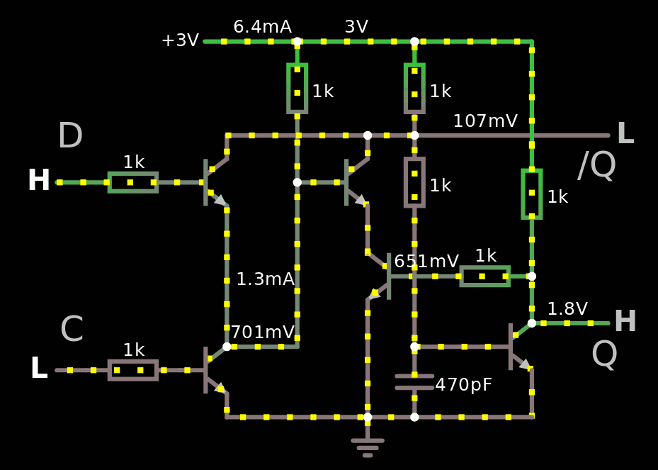
So here is a new version :
![]()
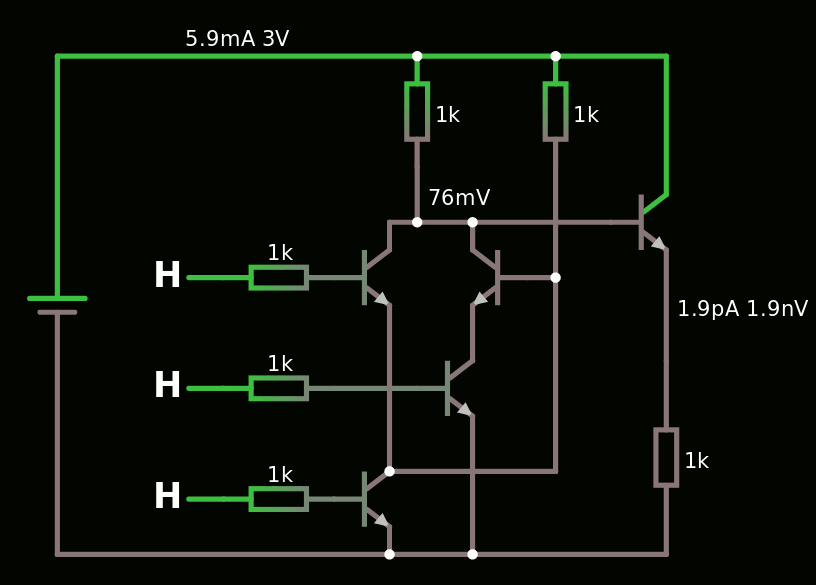
This one works down to 2V. It uses the same values for all resistors, it has a /Q output as well, a single-phase clock input, and only 5 transistors.
So far there are 5 transistors but for a whole register, the clock transistor can be shared among several bits.
At one point, I had to add a 1G resistor to prevent totally bonkers behaviour of the simulator between the two PN junctions of the transistors in series, ignore it for real circuits. In rare cases however, Falstad indicated 25GV at that node...
This time, I understood that there is one case that looks wrong but has no real effect on the circuit : when C is low and Din is high and feeds current into the /Q node, but it does not matter. In previous versions I added diodes to prevent current from flowing back but when absent, the working supply voltage can go lower and the noise immunity is better (or it can dissipate less power).
The /Q output might not be required. In this case, the 1K resistor that feeds the base of the output transistor could be omitted. This would also speed the circuit up a bit.
At some points I have problems with Falstad's sim (how surprising !) because the circuit wouldn't want to hold the High state on Q. I added a 470p capacitor to hold a bit of charge during the clock transition but later retries (and a full screen refresh) work without it... The value is approximate and the transistors' inherent capacitances would normally do the trick and add the tiny delay. Of course, a full simulation with xSPICE will work better :-)
Of course Falstad is a bit buggy but in practice, it's a lot like in real circuits, which are not perfect either. If you can make your circuit work in many conditions in Falstad's sim, the real circuit has good chances to work in real life.
The next step is obviously to create a DFF with a pair of these cells but in practice, timing is everything and with discrete computers, the clock strobe can be made very short, or successive latches can be strobed by clock signals with a little delay...
-
Analog Multiplexer Logic
04/10/2020 at 15:46 • 13 commentsNot all weird discrete logic has to be based on ancient components.
Most projects in discrete logic families focus on recreating ancient circuit styles (like RTL, DTL, DCTL or, as a bastard abberation, LTL) with the components that are still available today. It turns out that many of the specialized transistors are long gone. How about doing it the other way: Pick a minimal building block that is easily available today and base logic on that?
Browsing distributor listings I found an interesting category of small devices: Analog switches and multiplexers.
Basic building Block: The 2:1 Multiplexer
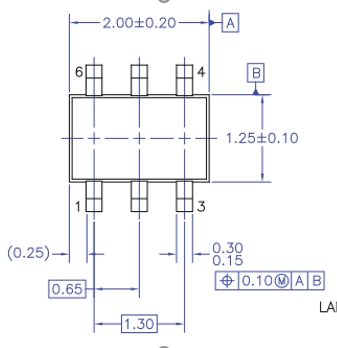
An example of an 2:1 analog multiplexer is shown above. These are not digital devices, but actual analog switches. The connection between B and A will be low ohmic when it is active and assume a very high resistance when deselected. This means that it can be used in both directions.
There is an abundance of 2:1 switches available in very small SOT-363 packages (above) from different sources for prices that rival that of discrete transistors. A short listing of some of the devices I found on LCSC is in the table below:
Part Manufacturer Price (100+) NC7SB3157 On Semi $0.046 74LVC1G3157 Diodes Incorporated $0.037 74LVC1G3157 Nexperia $0.048 SGM3157YC6 SGMICRO $0.03 BL1551 Shanghai Beiling $0.03 CH443K Jiangsu Qin Hang $0.036 SGM3157 Youtai Semiconductor Co $0.036
Spice Model
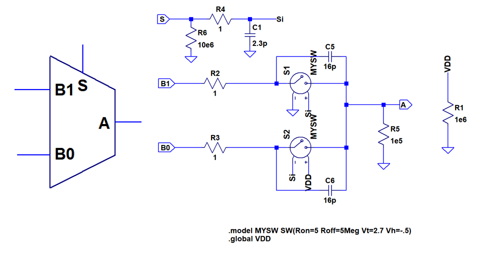
Unfortunately I was not able to find any spice model of these devices that is suitable for LTspice. So I made my own behavioral model as shown below, next to the entity symbol. Many parasitics are not considered here. Neither is the delay that the control logic is causing, so it can only be seen as a crude approximation.
Note the biasing resistor on the output, which is very important to prevent LTspice from getting stuck in a metastable state. Spice does not really like switches...Building basic logic gates
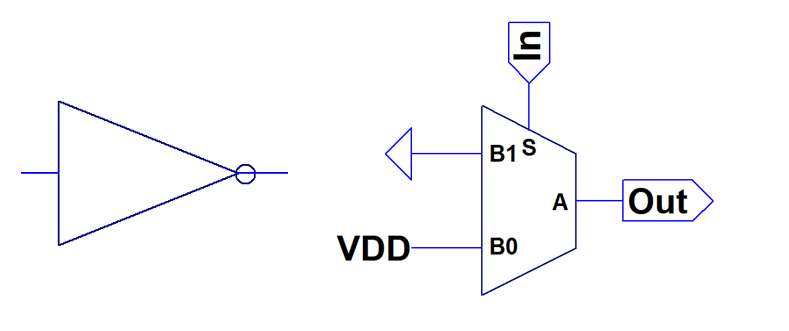
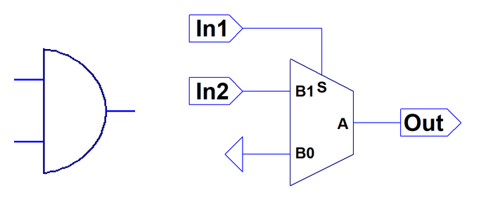
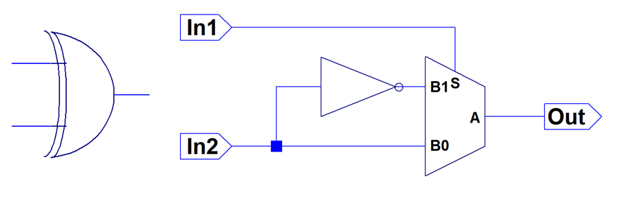
Most basic two-input gates can be realized with one or two analog multiplexers. It's interesting to note that the MUX is more accomodating to positive logic. Inversions typically require adding an additional multiplexer.
Inverter
AND Gate
The OR gate can be realized in a very similar manner. NOR and NAND require an additional inverter.
XOR Gate
XOR can be realized by an multiplexer that selectes between an inverted and non-inverted version of the secondary input. XNOR is realized by swapping multiplexer inputs.
Latches
Latches are the achilles heel of any logic family. Building a latch with a digital multiplexer is actually fairly easy and can be done with a single multiplexer by routing the output back to one of the inputs. However, this is not so easy with analog multiplexers, as they only act as a switch without any buffering or amplification.
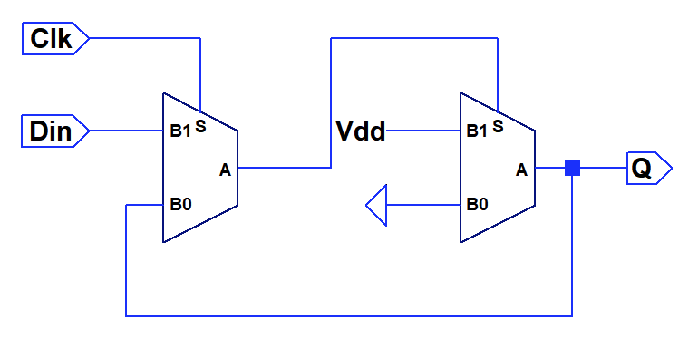
Instead, we will revert to a dynamic latch as shown below.
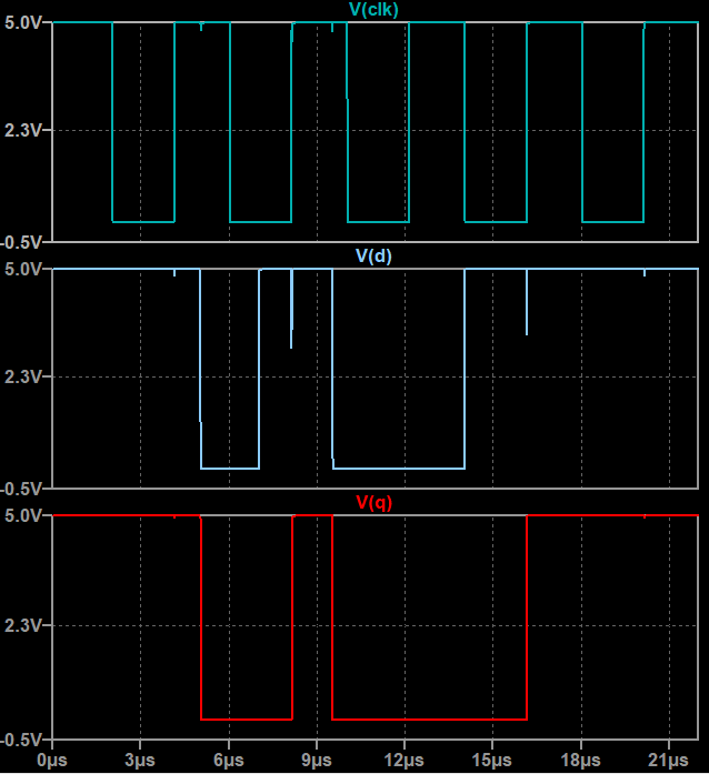
The first multiplexer acts as a path gate. If the clk is high, the input data will be routed to the output where the storage capacitor is charged. If the clk is low, the output will be connected to a floating input, so that the charge on the capacitor is held. The second multiplexer acts as an output buffer.
Obviously this is a bit tricky in operation as some of the charge will dissipate through leakage into the buffer control input and internal leakage in the multiplexer. A sufficiently high clock is required to allow cyclicated refreshing of the latch content.
The figure above shows simulation results of the latch in operation. Since loading of the capacitor causes a current surge on the input, spikes are seen on the input signal. Proper buffers and dimensioning of the storage capacitor is necessary.
Counter design
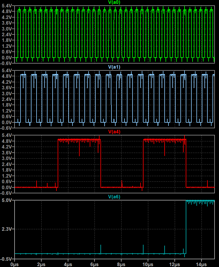
To verify the functionality in a more complex circuit, I designed an 8 bit counter in spice. You can see some of the output traces above. I hope that some of the transient spikes disappear once real-world parasitics are added.
Summary
This looks like a potential approach to build discrete logic from modern components. I have not yet tried real circuits, but will do so once I get around. The gate propagation delays could be quite acceptable as turn-on and turn-off times of the multiplexers listed above are in the sub 5ns range, according to their datasheets.
EDIT: Improved Latch
As Joan pointed out below, it is perfectly possible to turn the dynamic latch into a static one. This allows removing the capacitor. The circuit is basically the same as one would use with a digital multiplexer. However, since the analog switches don't have any gain in their signal path, we have to introduce a second switch that is used to buffer the signal and create gain in the hold loop. Circuit below.
-
Project proposal : Ring oscillators zoo !
03/14/2020 at 01:30 • 14 commentsWe TTLers love to test technologies, play with parts and explore new (or old !) realms. And one of the first things we do when we get our hands on a new transistor is see how fast they can go !
For example:
#Ring Oscillators: Fairchild DTL 949 by @Dana Myers
CBJT ring oscillator by @Ted Yapo
Relay ring oscillator
I2L ring oscillator by @Dana Myers
2N2369 ring oscillator / #Discrete Bipolar Logic (RTL/LTL) / Speed optimisation of pmbt2369 ring oscillator by @Tim
LTL ring oscillator by @Tim
Emitter-Coupled Logic ECL ring oscillator by @Dana Myers
74AC02 gated ring oscillator by @Ted Yapo
BC548B 5 Stage Ring Oscillator by @agp.cooper
Ring oscillators on Silego GreenPAK 4 by @whitequark ...
. (add yours here !)These days I'm contemplating "tasting" BFP740 (44GHz GBW but not in stock so far) and 2N2369 gates (I have a fistful but not enough to make anything interesting)...
I propose to create a new project/page where we gather all the ring oscillators experiments, sort them by technologies, discuss on measurement details (and gotchas) and agree on a standard "size" to help tally and compare speeds, efficiencies etc.
I was thinking that with my BFS480 (rated at 7GHz) I would need 9 inverters in series to have a reasonably observable waveform and a frequency that my HP5335A could accurately follow.
Is anybody interested ?
-
From MUX to Latch
01/31/2020 at 01:35 • 9 commentsEdit : this exploratory page is interesting but not the final word. The rest is logged at More bistables...
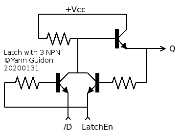
You know that a MUX can be easily turned into a latch by looping the output back to one input...And in From XOR to MUX I turn a XOR into a MUX. So the next logical step is to connect the output to one of the inputs...
![]()
The natural choice is to connect Y to A because the polarities are compatible.
This is unfair for the /B input which is inverted and requires a pull-down transistor.
![]()
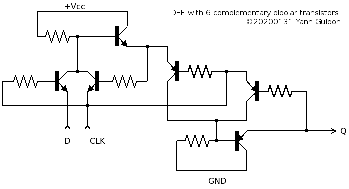
My quest is to make a D-FlipFlop circuit with the least number of bipolar transistors. A pair of latches will require another NPN to pull /D low, but another topology is possible if complementary transistors are allowed :-) As in the early IBM ECL circuits (Current Steering Logic) I can make the next stage complementary to save one transistor... As a bonus, there is no need of a complementary clock signal and the output data has recovered its original polarity :-D
![]()
Now, the more I look at it, the more I doubt it can work as is. There must be errors here and there...
I'm sure the CLK signal will create quite a lot of problems and it must be split into overlapped, out-of-phase signals (2-phase clock ?)
But I'll have to test and you know, you're never safe from a good surprise... who knows if it could be the basis of a new clock or UART ?
Edit :
@roelh commented :
- Normally, both transistors must invert the signal, but in your circuit one of them is an emitter follower that does not invert.
"yes but" double inversion is not the real requirement for latching, it's a consequence that transistors can only invert. We can apply the https://en.wikipedia.org/wiki/Barkhausen_stability_criterion which states : gain > 1 and phase = 0 (mod 2Pi). To fulfill this condition, you need 2 transistors because each adds a phase of Pi, and their gain is >1. However, most latches are used both in common emitter configuration, which creates the double inversion. Here I use another structure, similar to a SCR https://en.wikipedia.org/wiki/Thyristor
![]() "It acts exclusively as a bistable switch, conducting when the gate receives a current trigger, and continuing to conduct until the voltage across the device is reversed biased, or until the voltage is removed" because I use the common collector output (borrowed from the classic ECL gates structures). My circuit is almost identical, I only added a base resistor to prevent damage and too hard a saturation. The phase is 0 and the gain is very high so latching should occur as long as the CLK level is enough (which will be another concern for later)
"It acts exclusively as a bistable switch, conducting when the gate receives a current trigger, and continuing to conduct until the voltage across the device is reversed biased, or until the voltage is removed" because I use the common collector output (borrowed from the classic ECL gates structures). My circuit is almost identical, I only added a base resistor to prevent damage and too hard a saturation. The phase is 0 and the gain is very high so latching should occur as long as the CLK level is enough (which will be another concern for later)- Personally I would design a transistor CPU in such a way that the registers are latches (that was also done by Dieter in his transistor CPU).
I agree too : this cuts the transistor count in half and this is what is intended for #YGREC8.
However it is necessary to see the full DFF working on the bench and be familiar with its idiosynchrasies, before I cut it in half. It's important because I'll have to decide which part is NPN and which part is PNP. Apparently here the first/common latch is PNP because there are fewer transistors, and the bulk (replicated for each register) would be NPN because I have more of these.
The speed and timing of the circuit will depend on the power supply, the saturation and other parameters... I might have to add a anti-saturation diode in the SCR latch part, while the saturation of the emitter might not be such a problem. In fact, saturation is often considered in common emitter configurations, but here the emitter is a data input so I'm in a totally uncharted territory...
And I would love to test the circuit in both Silicon and Germanium versions. I don't have Germanium NPN transistors though (or so few, eventually) so it would be interesting to find a solution with only a single type/polarity.
Time to play with Falstad !!!
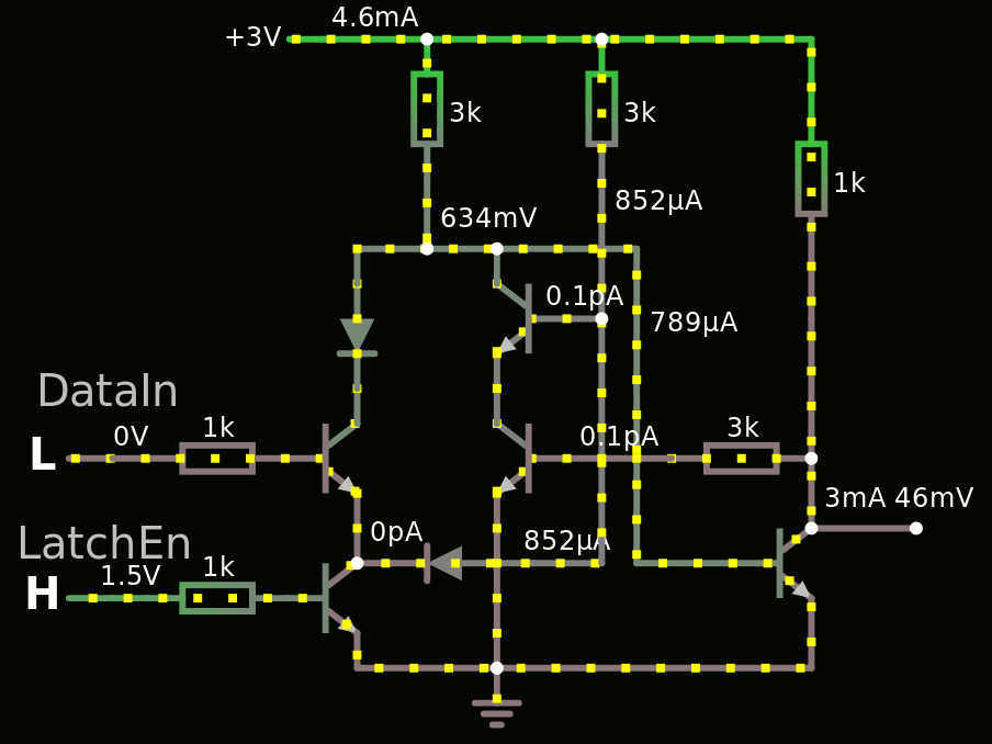
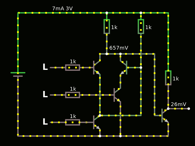
So I played with Falstad for hours and came up with this simulation :
![]()
The code :
$ 1 0.000005 0.11813604128656459 59 5 43
w 256 112 304 112 1
r 304 112 304 176 0 3000
t 240 304 272 304 0 1 -0.6341321488431279 -0.028103041567142044 100
t 368 240 336 240 0 1 -0.1887122097919851 0.04999867754124937 100
t 368 304 336 304 0 1 -0.34921107400413387 0.046210209898701 100
r 384 112 384 176 0 3000
r 176 304 240 304 0 1000
w 304 176 304 208 2
w 272 288 272 272 0
w 272 208 304 208 0
w 304 208 336 208 0
w 336 208 336 224 0
w 336 288 336 256 0
L 160 304 128 304 0 0 false 1.53 0
L 160 368 128 368 0 1 false 1.53 0
w 272 352 272 320 1
w 352 352 384 352 1
w 384 240 384 352 0
t 240 368 272 368 0 1 0.5923557570386799 0.6204587987064846 100
w 304 112 384 112 0
w 384 192 384 176 1
w 272 400 272 384 0
w 400 208 336 208 0
r 176 368 240 368 0 1000
t 400 352 480 352 0 1 0.5879219616224369 0.6341321712360694 100
w 384 112 480 112 0
w 480 240 480 304 0
r 480 112 480 240 0 1000
w 480 336 528 336 0
w 400 208 400 272 1
w 480 368 480 400 0
x 125 280 191 283 4 20 DataIn
x 116 350 197 353 4 20 LatchEn
w 480 336 480 304 3
r 416 304 480 304 0 3000
d 272 224 272 272 2 1N5711
w 272 208 272 224 0
d 352 352 272 352 2 1N5711
w 384 192 384 240 0
w 400 272 400 352 0
w 368 304 416 304 1
w 160 304 176 304 2
w 160 368 176 368 2
w 368 240 384 240 1
w 480 400 336 400 0
w 272 400 336 400 0
w 336 320 336 400 0
g 336 400 336 416 0
R 256 112 224 112 0 0 40 3 0 0 0.5
38 13 2 0 3 A\sLow
38 13 1 0 3 A\sHigh
38 14 2 0 3 CLK\slow
38 14 1 0 3 CLK\shigh
Note that the diodes are not standard, but low-drop Schottky, or else the bases can't be pulled down low enough. Or else another diode must be added to the output transistor's base...
I've also had strange problems with the inputs going all the way up to 3V. This seems to be solved with the 0-1.5V range but this needs to be explored and explained.
Thanks again to @roelh for pointing my errors ;-)
There are still a lot of things to examine, for example if it's topologically equivalent to other circuits, and what the advantages & drawbacks are. One great part is the Latch Enable signal and transistor that can be shared with other cells, so there are 4 transistors that matter, and most cells also have 4 transistors (IIRC).
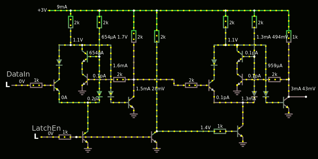
I've been able to make a full D-FlipFlop :
![]()
This version uses all-silicon standard parts, because I added a diode to the output's base.
From there I could build a shift register, which opens the door to Johnson counters, LFSRs, UARTs...
And here is a first attempt at a divide-by-two cell:
I had convergence problems and added a couple of 10M resistors.
I suspect there are 2 superfluous transistors to link the right latch back to the left...
In the end I chose a different method, that draws 2× less current and uses fewer parts. -
From XOR to MUX
01/17/2020 at 01:59 • 4 commentsYou might remember my musings with the XOR gate with interlocked NPN transistors discussed at Bipolar XOR gate with only 2 transistors
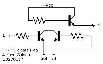
But thinking about how XOR is done with pass transistors in CMOS and the structure often creates a MUX, I wondered if I could translate this concept back to bipolar world.
![]()
This first result is pretty nice and compact though the circuit is highly unbalanced...
- A is a typical high-impedance input where a high signal is a valid 1.
- /B is a negated low-impedance input that must be shorted to -V to make a valid 1. Another transistor can do the trick though that would create another delay...
- Sel has to swing High and Low...
But for discrete, parts-constrained circuits, that might work...
The output could be used to directly drive another MUX stage if the next MUX swaps the NPN for PNP (and reverse polarity) though a big MUX could also be built with the single-transistor NPN-ANDN gate to then drive a big CTL AND gate.
Has anyone seen this circuit before ?
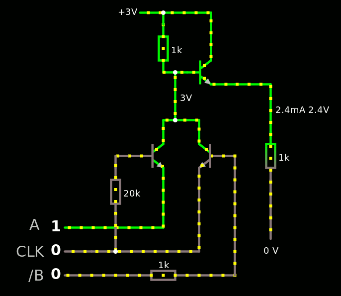
The MUX seems to work well on this Falstad simulation:
![]()
Another Falstad sim was required to validate the enhancements : an additional transistor to de-invert /B can be useful...
![]()
The source code is :
$ 1 0.000005 10.20027730826997 50 5 43
w 144 112 352 112 3
v 144 400 144 112 0 0 40 3 0 0 0.5
r 352 112 352 176 0 1000
t 304 240 336 240 0 1 0.6163510467707772 0.6473024119705006 100
t 416 240 384 240 0 1 -0.030951365199723496 0.027087887962126838 100
t 352 304 384 304 0 1 0.6173128261844162 0.6352410780104729 100
r 432 112 432 176 0 1000
r 240 304 304 304 0 1000
r 240 240 304 240 0 1000
w 352 176 352 208 2
w 336 224 336 208 0
w 336 208 352 208 0
w 352 208 384 208 0
w 384 208 384 224 0
w 144 400 336 400 0
w 384 400 384 320 0
w 384 288 384 256 0
w 304 304 352 304 0
L 240 304 208 304 0 1 false 3 0
L 240 240 208 240 0 1 false 3 0
L 240 368 208 368 0 1 false 3 0
w 336 400 384 400 0
w 336 352 336 256 0
w 336 352 432 352 0
w 416 240 432 240 0
w 432 240 432 352 0
t 304 368 336 368 0 1 0.6161066110712008 0.6611227508593843 100
w 352 112 432 112 0
w 432 240 432 176 0
w 336 400 336 384 0
w 464 208 384 208 0
r 240 368 304 368 0 1000
t 464 208 496 208 0 1 -2.924032495012093 0.07596750308398237 100
w 432 112 496 112 0
w 496 112 496 192 0
r 496 288 496 400 0 1000
w 384 400 496 400 0
w 496 224 496 288 3
38 18 2 0 3 B\sLow
38 18 1 0 3 B\sHigh
38 19 2 0 3 A\sLow
38 19 1 0 3 A\sHigh
38 20 2 0 3 CLK\slow
38 20 1 0 3 CLK\shigh
I have re-wired the B base resistor : it's now a pull-up that is shorted to 0V by the main SEL input. I added another transistor on the B input to get rid of the inversion (and some isolation).
The output is inverted with an common collector output stage, though an open collector is also possible, it would re-invert the value and make it a non-inverting MUX.
The select input and transistor can be shared by more than one MUX, which makes it an attractive solution for selecting a whole bus for example.
Here is the non-inverting MUX with open collector output :
![]()
So this is the version that would solve the problem found by @roelh :-D
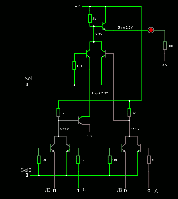
And when you have a MUX2, you can cascade 3 of them to build a MUX4 :-)![]()
There are inversions here and there but some are opportunities to save a transistor.
-
The return of CTL
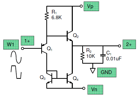
09/18/2018 at 16:37 • 0 commentsI found the original source of that story (ECL or CTL : what's the fastest topology for discrete gates ? [updated]) about "CTL" (Complementary Transistor Logic, which, since it doesn't invert, can't qualify as logic :-P ) http://www.6502.org/users/dieter/mt15a/mt15a_3.htm
The author presents his TTL gate, then his modification inspired from TTL.
![]()
I did some tests and tried a basic gate and... "it's a weird AND".
More precisely it works as a linear amplifier with close to no voltage gain but strong current gain. When the circuit is rewritten, it's obviously a pair of complementary "emitter followers" with the output clamped above 2.5V-Vbe=1.7V. The output can go down to about 0.2V on my tests.
This circuit also has a strong tendency to oscillate. My test setup was poorly designed but I could stop 60MHz oscillations with a 4n7F capacitor at the input of the PNP. I'll see how I can get a stable circuit...
Since this is just a pair of emitter followers, why bother with using PNP inputs after all ? With my BC559C, each with hFE=480, the overall gain is about 200K, the input current is very low but this is overkill and oscillations are not surprising at all.
The PNP emitter followers at the input are nice. The NPN emitter follower at the output is nice. AND gates are very useful in some places. However this is not what we expect from a "logic gate" because there is no real "active level" or "threshold". Current gain is nice but voltage gain is important too ! So this CTL might be faster than ECL but ECL can do more functions and provide inversion.
Furthermore, it looks quite a lot like the Low Offset Emitter Follower :
![]()
After this little setback (or disappointment) I looked at other ways to make this circuit and a variation appeared : it replaces selected PNP input transistors with NPN.
Thus instead of inverting the output, we can invert the necessary input(s) and we apply "bubble pushing" :-)
Of course the logic levels are modified but this leads to the interesting concept of a cascade of emitter followers, "or-dotted" together for the OR functions, with parallel transistors for AND or OR functions, and complementation (switching from PNP to NPN and vice versa) for the negation.
Of course we can also use BJT as ANDN gates :-)
-
Bipolar transistors are ANDN gates !
09/10/2018 at 12:41 • 3 commentsIn the log Bipolar XOR gate with only 2 transistors we see the legendary interlocked transistor gate :
![]()
Then this HAD post describes a very clever driving scheme :
![]()
Then it became clear... Under the right driving situation, a transistor (with its base resistor) is a ANDN gate !
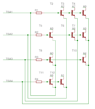
Why does it matter ? Because this could greatly help to implement circuits such as this 7-segments decoder:
![]()
This is a sort of "slow" circuit where parts count matters more than speed (hard saturation is not an issue) so hacks like this will help a lot :-)
For the above "arbitrary logic" array, wired-oring will also save parts. All we have to do is "solve/reduce with ANDN". Who wants to play that game with me ? :-D
-
The rule of 50 (or so)
09/10/2018 at 12:27 • 10 comments[updated 20180930, read the comments below for more background]
People usually confuse the operating frequency of the computer with the max. frequency of its individual parts.
Let's say a CPU runs at 1GHz, that must mean each transistor switches 1 billion times per second, right ? Hahaha I'm kidding.
Actually the Ft (transition frequency) of transistors is way higher than that. And the whole circuit is slowed down by other factors such as wires, capacitances, resistances that make distributed RC networks along with the capacitances, and countless other factors. Of course, the CDP (critical datapath) length matters too.
But in average, I have observed a 1:50 ratio between the operating frequency of a processor versus the "speed" of the constituting transistors, for reasonable architectures. This might be lower for recent ultrapipelined processors but when you make your own discrete processor, divide the Ft by 50 to get your final processor's speed. A ratio of 100 is much more realistic for a hobby project but it's less optimistic...
The ratio of 50 is a realistic ceiling that shows the influence of parameters outside the transistor's ideal characteristic. One such influence is the type of logic gate (TTL, DTL, CTL, DCTL, ECL...) so you have to measure your individual inverter gate speed (for example with a ring oscillator) for a better estimate.
I'd be happy to get more datapoints from various architectures and implementations. A chart would help us identify the factors that inflate or decrease this ratio and give us a better prediction.
Note : this rule applies to transistors and semiconductors, not relays, where the delay is limited essentially by the contact switching speed and RC delays are irrelevant.
-
Video Explaining DEC R-Series DTL
09/07/2018 at 03:40 • 3 commentsHey! I have made a short home-made video explaining an alternate form of DTL.
Click on the image below to view the video!
Video URL: https://tube.bootlicker.party/videos/watch/ae913c76-4540-4e14-b584-f5c16660dadc
~vidak
-
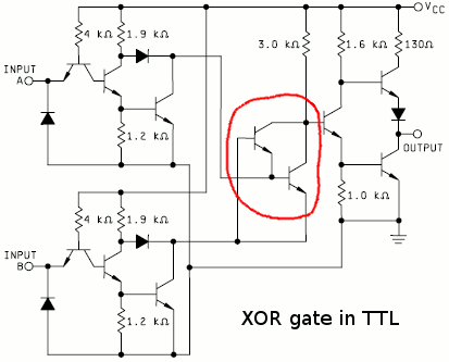
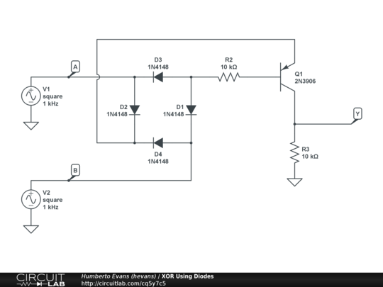
Bipolar XOR gate with only 2 transistors
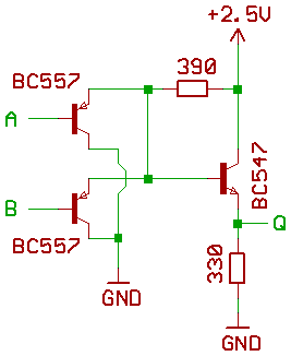
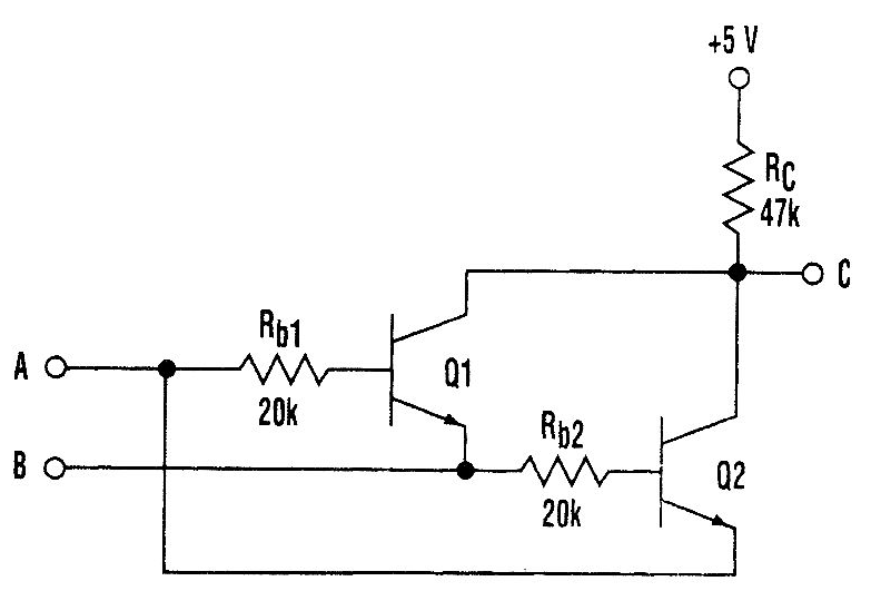
07/29/2018 at 15:49 • 48 commentsI sometimes find a small circuit with 3 resistors and 2 transistors that performs the eXclusive OR operation.
![]()
These two interlocked transistors use a very unusual structure, which requires the least theoretical number of switching elements, but it depends on a trick : the input impedances matter a lot and the circuit depends on a "hard" 0 level, because the circuit behaves almost like a "pass" element...
![]()
Thus, the question : is it the best method ? What about the switching speed or the capacitances ?
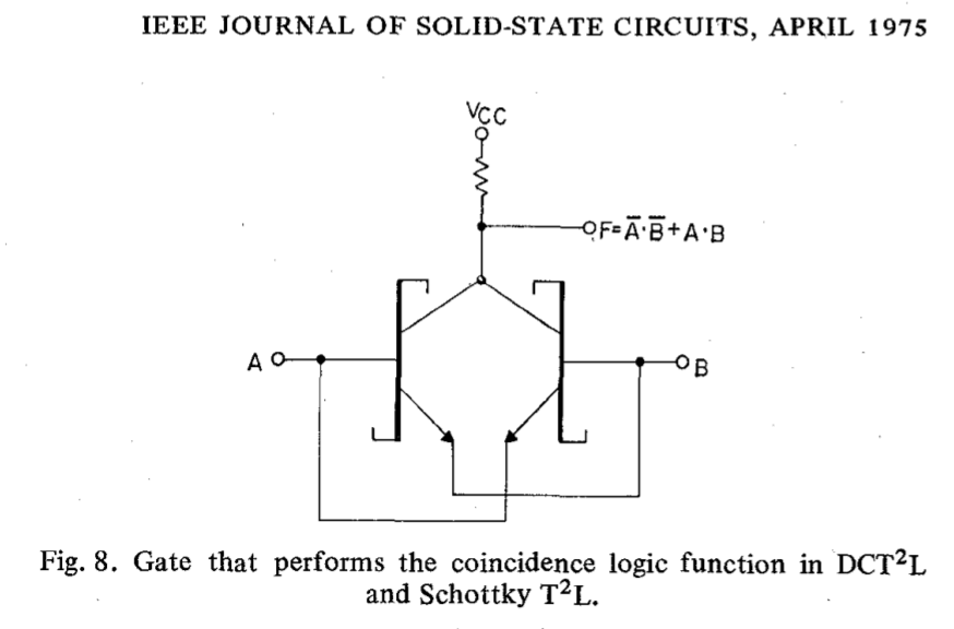
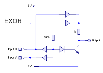
XOR is pretty important in CPUs because many mechanisms rely on it, for example ALUs. Does the gain in parts count affect the performance ? Apparently, it's pretty close to ideal because it's touted as a solution in Direct Coupled Transistor Transistor Logic:
![]()
Another version has only one transistor but 4 diodes :
![]()
This is more or less what Rory does :
Another question is : can this scheme (no amplification, just relying on the input's strength) be extended to other logic or sequential functions ?
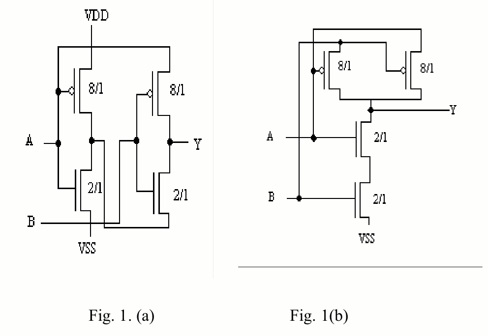
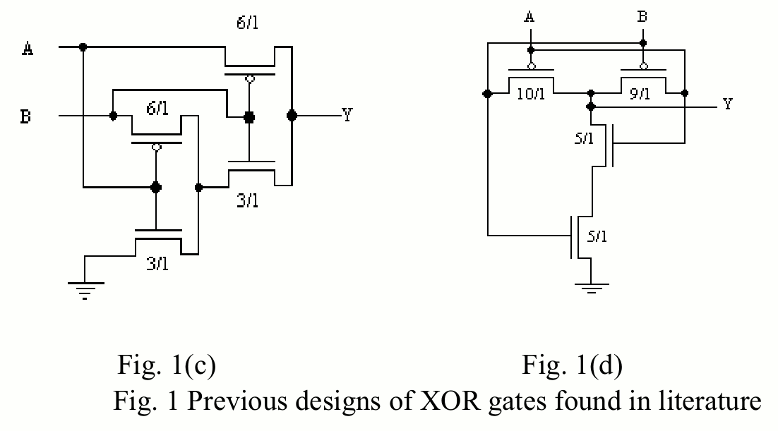
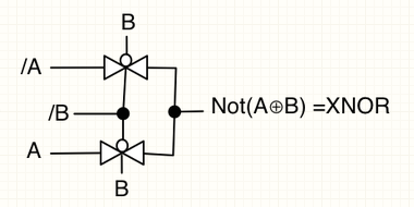
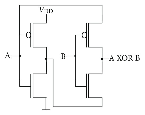
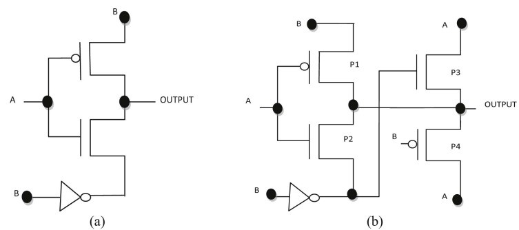
The XOR gate has a much wider range of implementations in MOS and CMOS. You can find circuits using 4, 6, 8, 9, 10 or 12 transistors, again with varied strengths for the inputs and the output. For example, pass-transistor logic (transmission gates) makes it pretty simple :
![]()
Each pass element is a pair of complementary transistors, so this gate uses 2 NMOS and 2 PMOS. Add as many if you want to isolate the outputs with inverters...
![]()
Oh and don't forget another inverter at the output. This is why you'll find various transistor counts. Unless the designer wants to decompose the function into elementary boolean functions, and the size explodes, depending on how you break it up:
![]()
![]() (also missing : picture with MUX2 and an inverted input)
(also missing : picture with MUX2 and an inverted input)This decomposition leads to the "classic" CMOS XOR gate:
![]()
which gains weight again when the inputs are buffered and inverted :
![]()
XOR has a reputation of a "slow and large gate" for this reason and that's why I investigate smarter topologies and their compromises.
Another version is also pretty nice :
![]()
This is interesting for my #Yet Another (Discrete) Clock because it is almost suitable for MOSFETs. The B input must double the transistors because of the inherent diodes but it's "only" 3×BS170 and 3×BS250. In this case, the B input actually works as a multiplexer or transmission gate... Which means it might not be suited for ultra high speed.
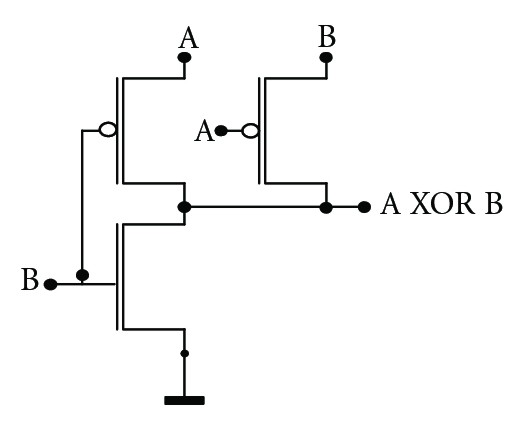
Even fewer parts with this 3T XOR :
![]()
In this case, only 1×BS170 and 3×BS250 are required. It's still not ideal because the BS250 is more expensive than the BS170 but I don't see how to permute the polarities without requiring more inverters... Furthermore, there seems to be a conflict with one of the input combinations : B=1 forces the output to 0, but if A=0 then the input B (which is =1) is forced to 0 by itself... The solution is another PFET controlled by A, in series with the grounding NFET.
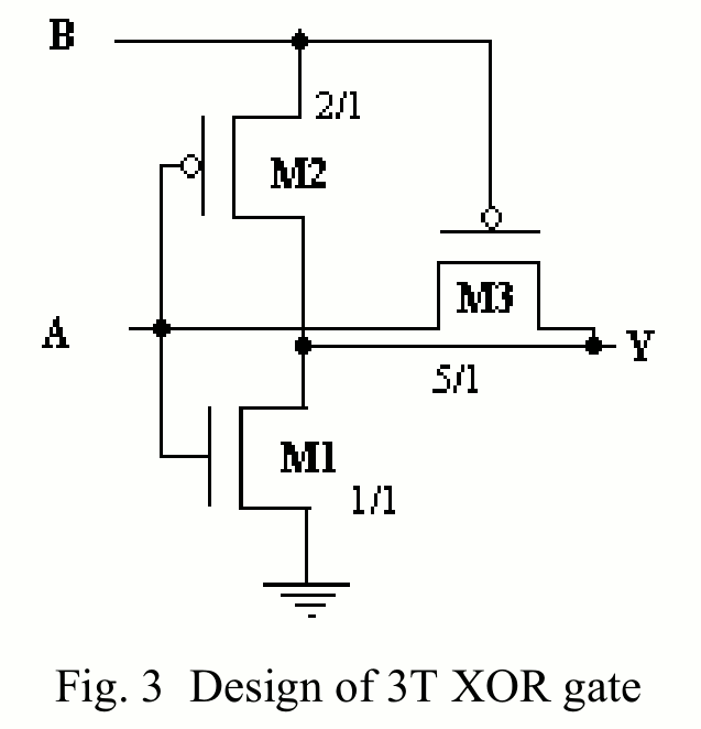
Another source https://waset.org/publications/1588/a-high-speed-8-transistor-full-adder-design-using-novel-3-transistor-xor-gates explains in great detail why the short circuit is not such a big deal for ICs : they tune the width/ratio of certain transistors to minimize the unwanted current. This trades space for power consumption.
![]()
M1 has a 1/1 ratio, almost a square, wih minimal size, hence highest resistance, while M3 has a high ratio to overcome the pull-down from M1. For very high-speed CMOS circuits, where power is dominated by switching (and leakage for the newest processes) this short current can be considered "negligible".
Another interesting compromise uses only 2 of each type:
![]()
But the "upper pass trick" on input A might still need doubling of the P-MOSFET to cancel the parasitic body diodes. This could be cheaper if XNOR was made instead, so 2 PFETs are tied to Vcc in series, and the NFETs are used as pass elements.
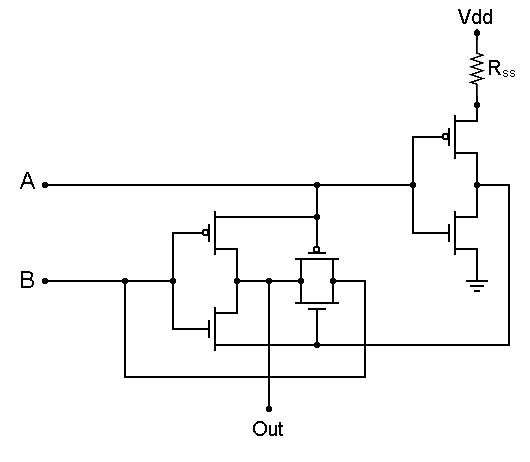
ICs use even more variations on these ideas:
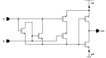
![]() This odd one seems to interlock the leftmost transistors, followed by a NAND and finally an inverter:
This odd one seems to interlock the leftmost transistors, followed by a NAND and finally an inverter:![]()
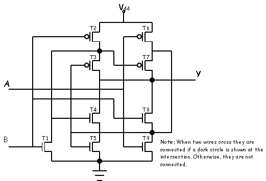
An enhanced 9T XOR:
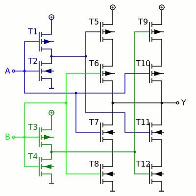
![]() Even more combinations with pass transistors :
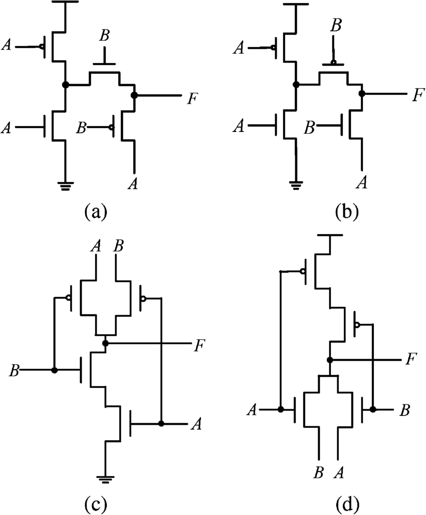
Even more combinations with pass transistors :![]() From https://waset.org/publications/1588/a-high-speed-8-transistor-full-adder-design-using-novel-3-transistor-xor-gates:
From https://waset.org/publications/1588/a-high-speed-8-transistor-full-adder-design-using-novel-3-transistor-xor-gates:![]()
![]()
But I have not seen such variety for bipolar circuits.
ECL can use some creativity as well but these gates require many transistors anyway so it's not as interesting.
I have however wondered how to modify the differential amplifier to perform this operation...
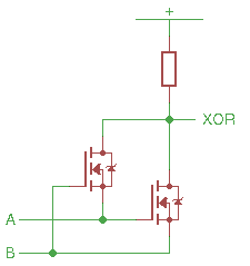
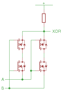
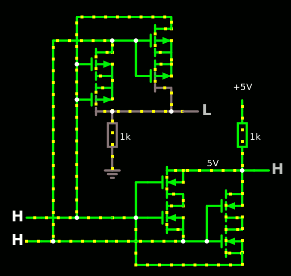
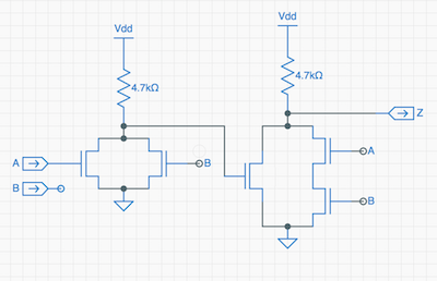
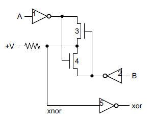
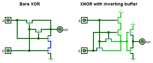
I still can't find an answer about the bipolar case but I could easily adapt the interlocked system to MOSFET, in a bid to avoid P-MOSFETs. Naturally, this gives :
![]()
A rough simulation shows that there is a conflict through the parasitic body diode when the inputs are opposite.
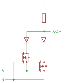
One cheap way to avoid this case is with the insertion of diodes in series, to prevent one input from shorting into the other :
![]()
Here is the simulation with Falstad.
or for the purists : cancel the body diodes with back-to-back N-MOSFETs :
![]()
It would work at a lower supply voltage and the simulation shows the low state has a lower voltage but the speed would be 2x slower because the FETs in series double the ON resistance...
OTOH : if you want XNOR instead, just flip the circuit upside down and use P-MOSFET :
![]()
spudfishScott uses 5 NMOS for his XOR at https://hackaday.io/project/162814-the-spikeputor/log/157607-building-blocks-2-multiplexors-and-flip-flops:
![]()
Update :
Master Ken reverse-engineered the Z80 at http://www.righto.com/2013/09/understanding-z-80-processor-one-gate.html and found a NMOS XOR :
![]()
Hackaday TTLers
Where DIY DIP/SSI/MSI CPU makers meet and discuss other TLA (three letters acronyms)
 Yann Guidon / YGDES


 "It acts exclusively as a


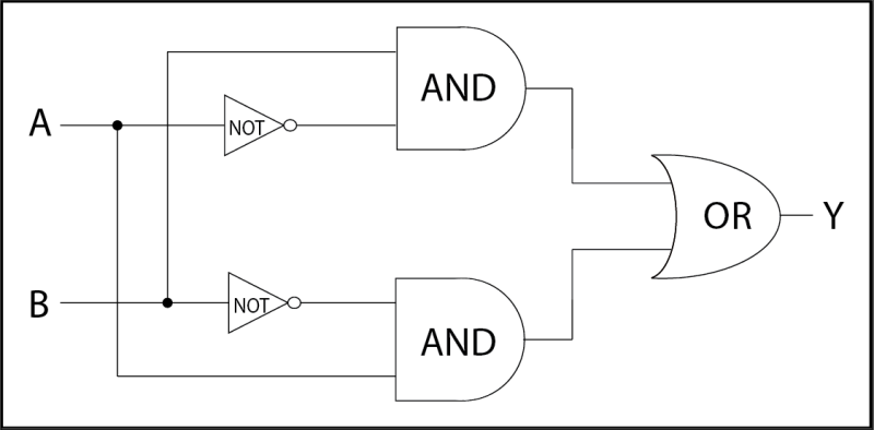
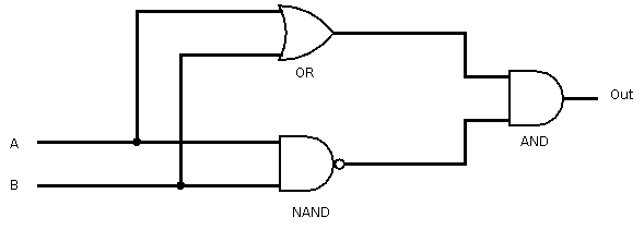 (also missing : picture with MUX2 and an inverted input)
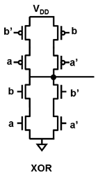
 This odd one seems to interlock the leftmost transistors, followed by a NAND and finally an inverter:
 Even more combinations with pass transistors :
 From
From 